Electronic design automation system and methods utilizing groups of multiple cells having loop-back connections for modeling port electrical characteristics

Inactive Publication Date: 2003-03-25
SYNOPSYS INC
View PDF5 Cites 184 Cited by
  • Summary
  • Abstract
  • Description
  • Claims
  • Application Information

AI Technical Summary

Problems solved by technology

Design, checking and testing of large scale integrated circuits are so complex that the use of programmed computer systems are required for realization of normal circuits.
This is partly because the integrated devices are inherently complex and partly because the circuit design needs to be decomposed into simpler functions which are recognized by the CAD tool.
A problem occurs in the prior art process of FIG. 1 in that the scan insertion process 213 does not take into account its impact on the mission mode design.
However, as is often the case, the addition of the testability cells by the scan insertion process 213 does not allow the second compile process 217 to meet constraints 205 without a design modification to the original HDL program 201.
It is disadvantageous to execute a second substantial compile process 217 in an attempt to match the testability cells and linking resources to the given set of constraints.
The addition of this second compile process, using conventional technology, delays the overall integrated circuit synthesis process by as much as one to two weeks.
In this case, a time consuming task of returning to the HDL for redesign is required.
Another problem faced by prior art designs involving the introduction of scan cells for testability while maintaining optimization constraints (e.g., timing and area constraints) is that the timing and area constraints cannot be met in some designs if the entire design is scan replaced.
Some memory cells do not offer a scan-in ability or do not offer a scan-out ability due to logic consideration

Method used


Image

  • Electronic design automation system and methods utilizing groups of multiple cells having loop-back connections for modeling port electrical characteristics
  • Electronic design automation system and methods utilizing groups of multiple cells having loop-back connections for modeling port electrical characteristics
  • Electronic design automation system and methods utilizing groups of multiple cells having loop-back connections for modeling port electrical characteristics

Examples


Example

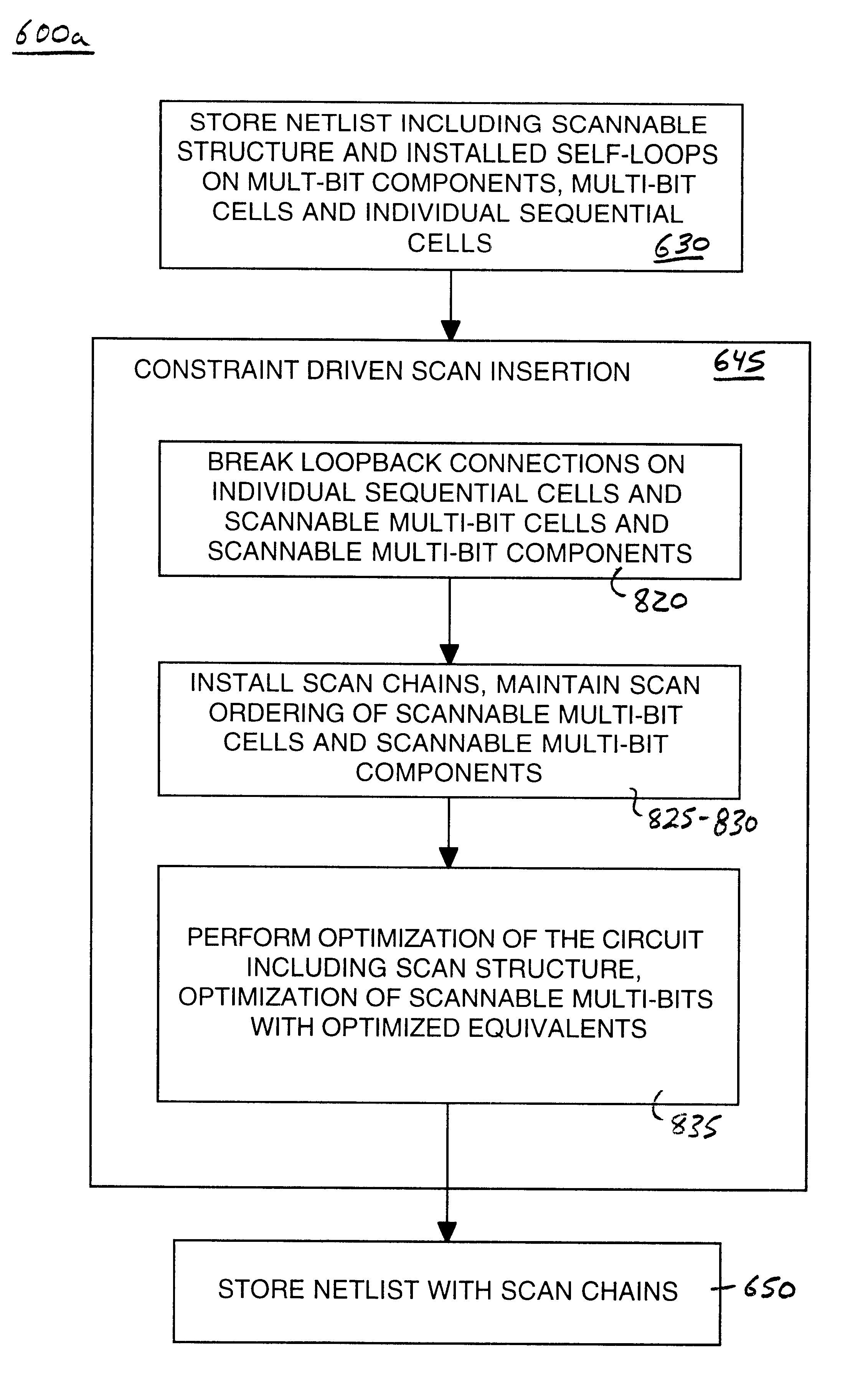
The loopback connections discussed above span between the ports of a single or individual scan cell and are called "self-loops." The following embodiment of the present invention, in addition to self-loops, also utilizes loopback connections that span from the scan-out port to the scan-in port of scans cells located within multi-bit cells and multi-bit components. Also used are long loopback connections that span over multiple individual scan cells (multi-cell groups). The loopback connections of multi-bit cells, multi-bit components and multi-cell groups act to simulate the electrical characteristics of the ports of scan cells as the ports would appear if coupled in a scan chain, thereby facilitating circuit optimizations, etc. As discussed above with respect to self-loops that span a single or individual sequential cell, multi-cell loopback connections provide the TR compiler 625 (FIG. 8) with enough information to determine the electrical impact of the DFT circuitry on its design...


PUM


Abstract

A computer implemented process and system for electronic design automation (EDA) using groups of multiple cells having loop-back connections for modeling port electrical characteristics. Multi-bit cells have multiple gates of the same function implemented within a same cell. Multi-bit components have multiple multi-bit cells implemented within a same component. Scannable multi-bit cells and components are similar to multi-bit cells and components but contain scannable sequential elements with scan chains installed. Multi-bit cells may or may not have each sequential cells' input and each sequential cells' output available externally. The scannable sequential elements of a multi-bit component are ordered into a predefined scan chain which is defined by the library containing the multi-bit component or multi-bit cell. During scan replacement processes of the EDA compile process, multi-bit cells and components of the netlist are replaced with scannable multi-bit cells and components. Also, during optimization, multi-bit cells and components undergo equivalence replacement to meet specified constraints (e.g., area, performance, etc.). To model the electrical characteristics of the port during certain optimizations, loopback connections are applied to the multi-bit components from the scan out port to the scan in port of the multi-bit cell or component, therefore, one loopback connection spans multiple sequential cells within the multi-bit cell or component. During certain optimizations, loopback connections are applied to multiple sequential cells that are coupled together but do not necessarily reside in a multi-bit cell or component. By spanning multiple sequential cells, circuit degeneration is reduced thereby providing better circuit optimizations for netlists having scan circuitry.

Description

(1) Field of the InventionThe present invention relates generally to the field of logic synthesis for integrated circuit devices. More particularly, aspects of the present invention relate to methods and apparatus for design for test within a logic synthesis system.(2) Background of the Related ArtComplex integrated circuits are designed with the use of computer aided design (CAD) tools. Specifically, application specific integrated circuits (ASICs) and field programmable gate array (FPGA) circuits can be designed using a variety of CAD tools. The development of ASICs and FPGA circuits with the aid of CAD tools is referred to as electronic design automatic or EDA. Design, checking and testing of large scale integrated circuits are so complex that the use of programmed computer systems are required for realization of normal circuits. This is partly because the integrated devices are inherently complex and partly because the circuit design needs to be decomposed into simpler functions...

Claims


Application Information

Patent Timeline
IPC IPC(8): G06F17/50
CPCG06F17/5045G06F30/30
Inventor SINGH, HARBINDERMARTIN, DENISAJJARAPU, SRINIVASWALKER, ROBERT
Owner SYNOPSYS INC
Why Eureka
Try Eureka