

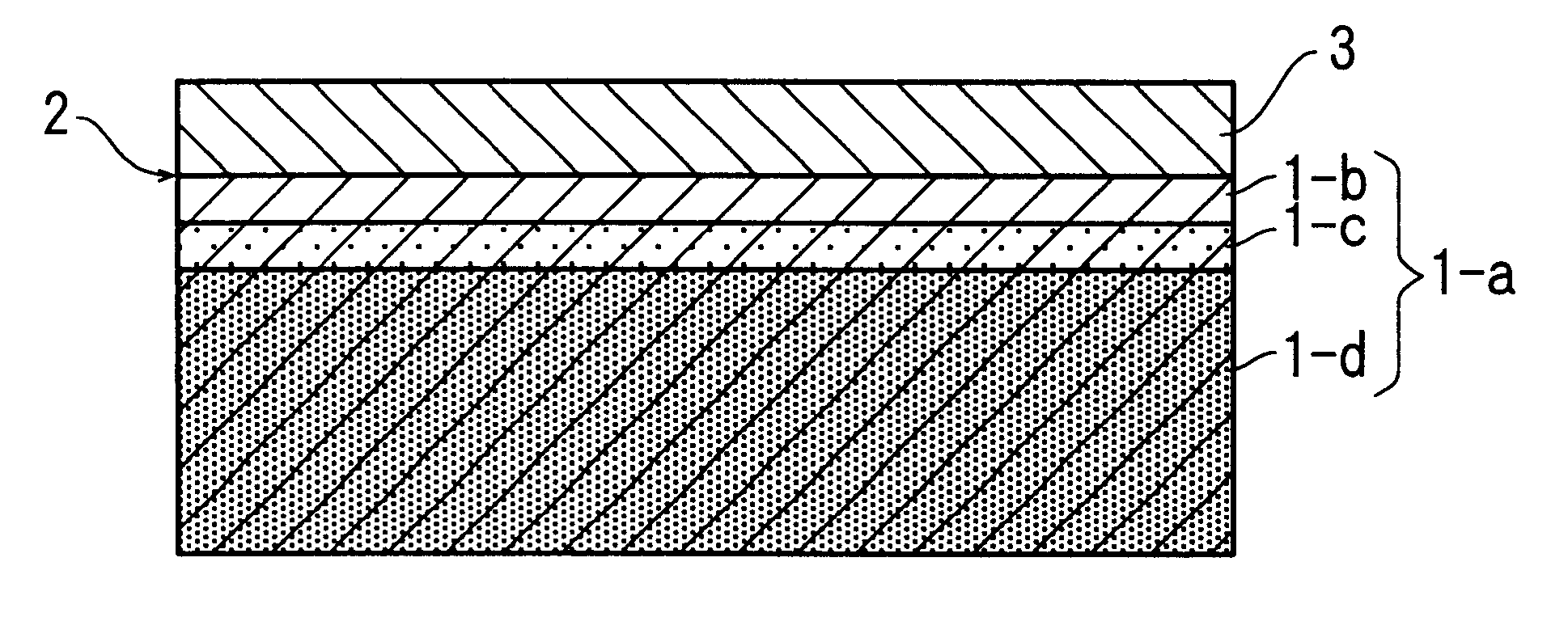
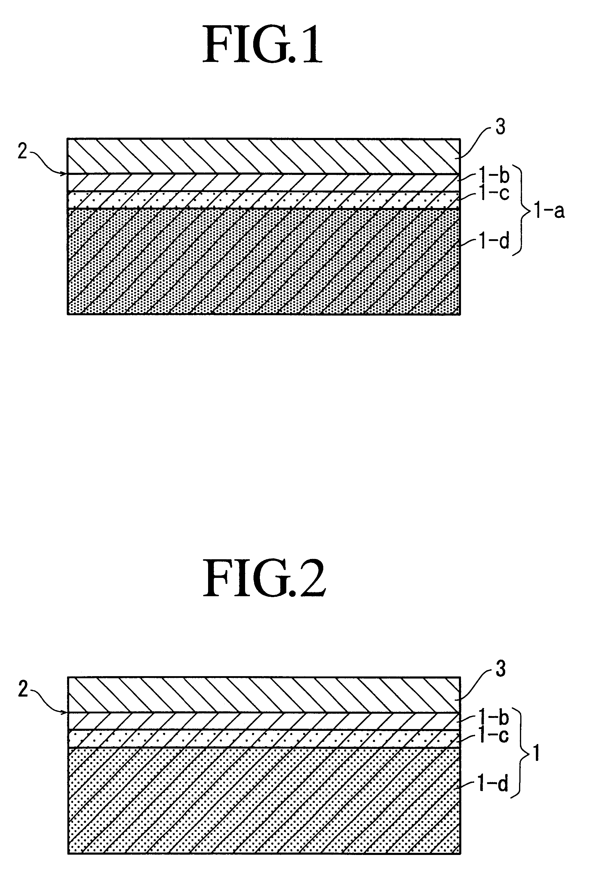
Silicon semiconductor wafer and method for producing the same
a technology of silicon semiconductor and semiconductor wafer, which is applied in the direction of crystal growth process, polycrystalline material growth, under a protective fluid, etc., can solve the problems of lowering the yield of devices, and affecting the performance of devices
- Summary
- Abstract
- Description
- Claims
- Application Information
AI Technical Summary
Benefits of technology
Problems solved by technology
Method used
Image

Examples
examples
Now, this invention will be described more specifically below based on working examples. It should be noted, however, that this invention is not limited in any respect by these working examples.
referential examples 1-8
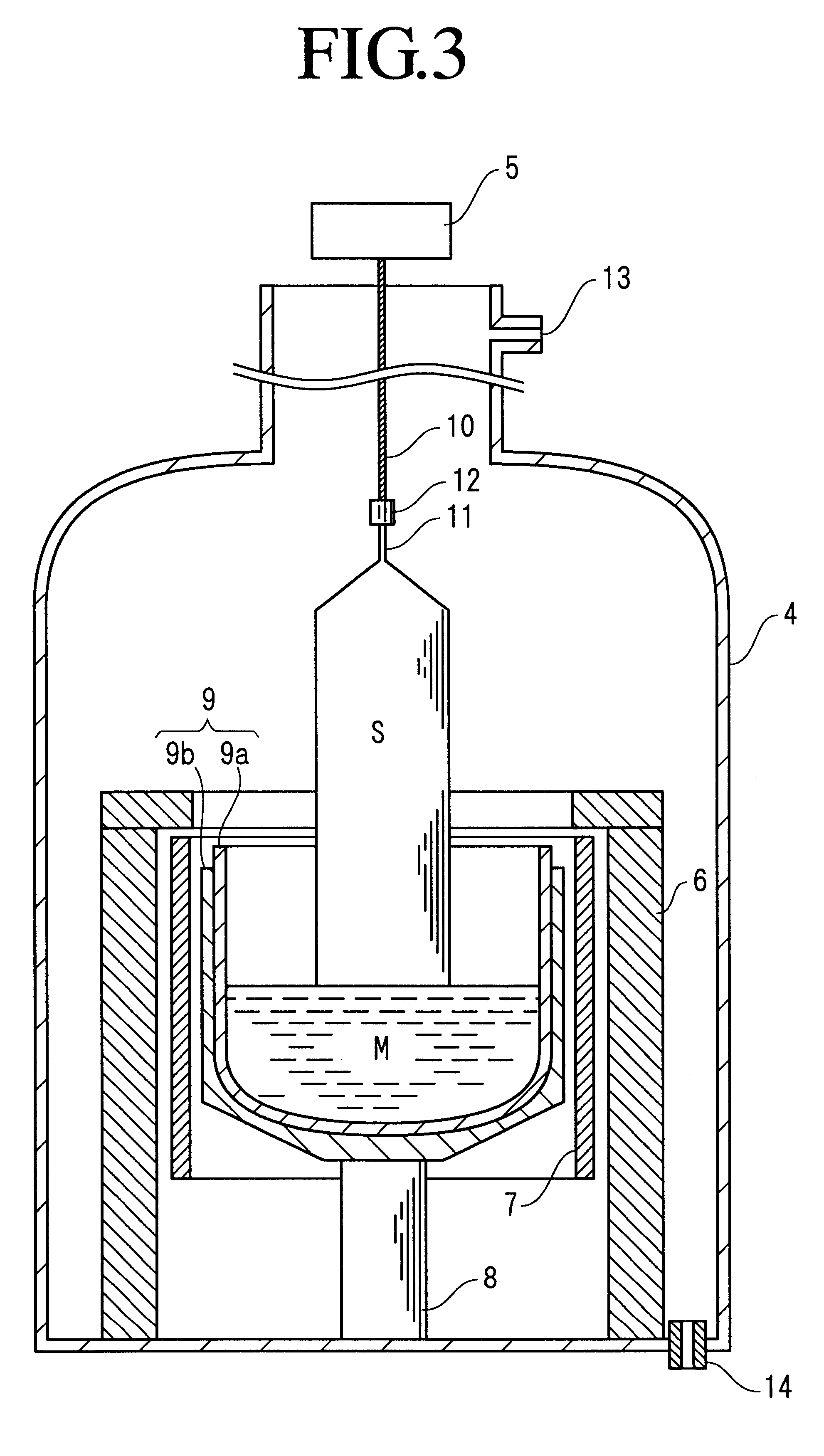
By way of referential examples, the following eight crystals were pulled by the Czochralski method. The oxygen concentrations of these crystals were in the approximate range of 6.5-8.5.times.10.sup.17 atoms / cm.sup.3 (determined by the infrared absorption method using the JEIDA conversion factor). They were invariably P-type 10 .OMEGA.cm crystals which were obtained by melting respective raw materials each weighing about 40 kg and pulling the molten masses into ingots, 155 mm in diameter and about 30 kg in weight. The doping of nitrogen was effected by preparing a wafer having a nitride film formed by the CVD method on a non-dope silicon crystal and dissolving the wafer at the same time that the relevant raw material was dissolved.
1) A crystal, adding no nitrogen, was grown by pulling at a speed of 1 mm / min.
2) From a raw material prepared in a molten state having added nitrogen at a concentration of 7.times.10.sup.15 atoms / cm.sup.3, a crystal was grown by pulling at a speed of 1 mm / m...
example 1
The wafers of Referential Example 5 and Referential Example 7 were heat-treated under the conditions according to this invention. They were inserted into a furnace at 800.degree. C., then heated at a temperature increasing rate of 10.degree. C. / min to 1100.degree. C., retained at this temperature for 8 hours, and left cooling at a temperature decreasing rate of -10.degree. C. / min to 800.degree. C. The substrates consequently formed were extracted from the furnace. The gas used for the heat treatment was obtained by receiving argon gas supplied by a cold evaporator and treating it with a purifying device at the point of use. This gas contained impurities at a concentration of not more than 5 ppm. This gas was passed through the site of the heat treatment mentioned and used as an atmosphere for the heat treatment. The substrates, prior to the insertion into the furnace, were purged with a purge box installed in front of the furnace. After the atmosphere keeping the samples waiting in ...
PUM
| Property | Measurement | Unit |
|---|---|---|
| thickness | aaaaa | aaaaa |
| temperature | aaaaa | aaaaa |
| temperature | aaaaa | aaaaa |
Abstract
Description
Claims
Application Information