Point diffraction interferometric mask inspection tool and method

a mask and interferometric technology, applied in the field of point diffraction interferometric mask inspection tools and methods, can solve the problems of complex masks using phase-shifting and opc, difficult inspection of masks, and degrading image resolution, etc., and achieves the effects of reducing the number of apertures of condenser and collector lenses, reducing the resolution of images, and reducing the resolution of masks

Inactive Publication Date: 2003-05-06
INTEL CORP
View PDF2 Cites 42 Cited by
  • Summary
  • Abstract
  • Description
  • Claims
  • Application Information

AI Technical Summary

Problems solved by technology

However, when the minimum critical dimension (CD) becomes smaller than the exposure wavelength, the resolution of the images is degraded by the spreading effects of diffraction.
Masks using phase-sh...

Method used


Image

  • Point diffraction interferometric mask inspection tool and method
  • Point diffraction interferometric mask inspection tool and method

Examples


Embodiment Construction

In the following description, numerous particular details, such as specific materials, dimensions, and processes, are set forth in order to provide a thorough understanding of the present invention. However, one skilled in the art will realize that the invention may be practiced without these particular details. In other instances, well-known semiconductor equipment and processes have not been described in particular detail so as to avoid obscuring the present invention.

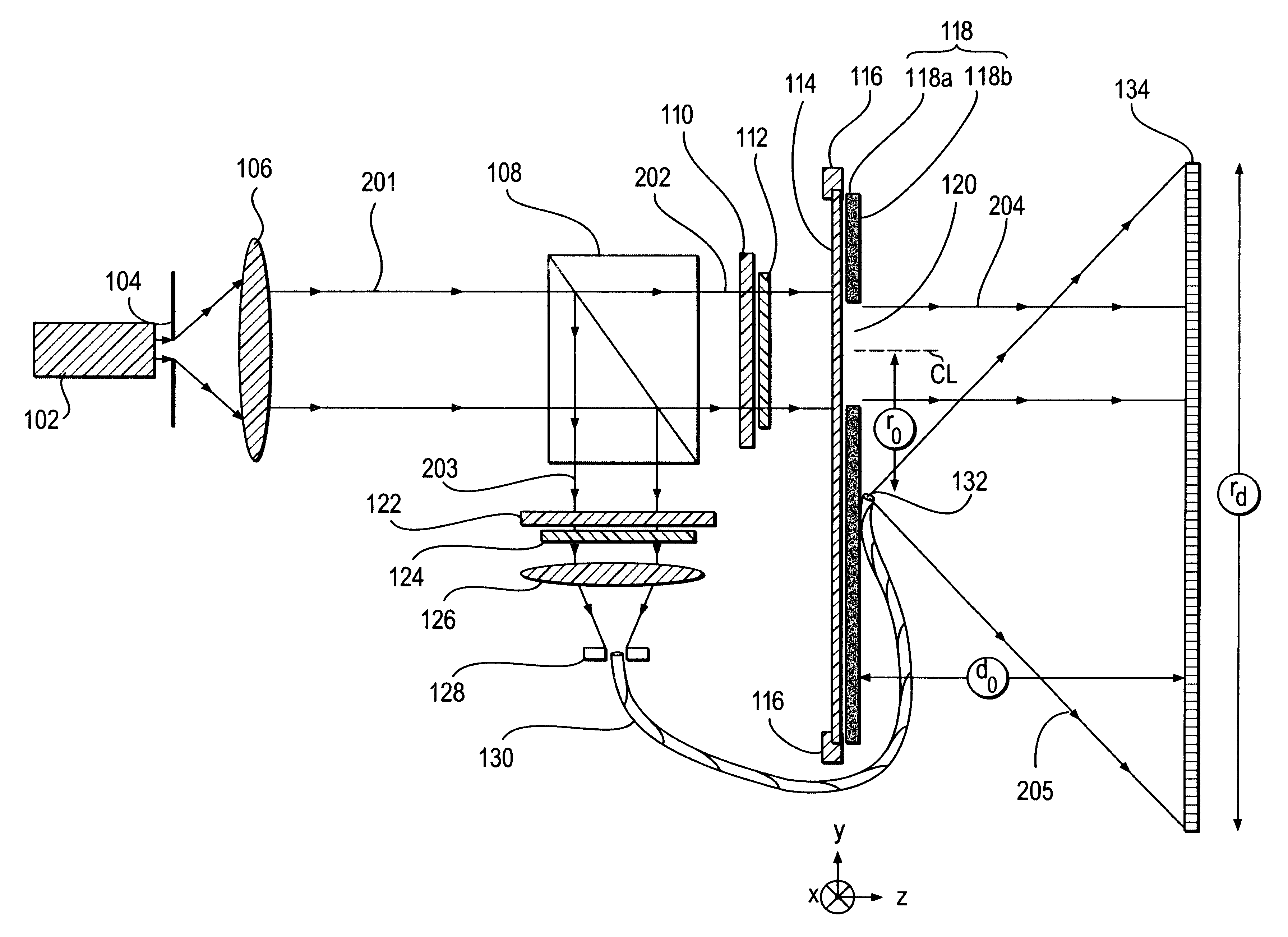
The present invention comprises a tool for and a method of inspecting masks used in photolithography. The inspection is performed using light with a central wavelength that is approximately the same as the actinic wavelength. The light is split into two linearly polarized beams which are orthogonal to each other and to the direction of propagation. The reference beam is an ideal spherical wave formed by diffraction through a pinhole. The test beam is a plane wave that has been transmitted through a transmissive mask ...


PUM


Abstract

The present invention comprises a tool for and a method of inspecting a mask used in photolithography to determine errors in phase, amplitude, and pattern edges. An embodiment of the tool comprises a laser source, a polarizing beam splitter, a first shutter, a mask, a second shutter, a quarter wave retarder, a single-mode optical fiber, and a CCD detector array. An embodiment of the method comprises four independent measurements of light intensity, comprising: a pattern of a mask, a diffraction pattern of a reference pinhole, an interference pattern of the mask and the reference pinhole, and an interference pattern of the mask and the reference pinhole with a known phase difference. Calculations are performed to determine phase and amplitude information as a function of location on the mask. The phase and amplitude information is then compared with a design layout of the mask to determine pattern edge information and identify possible defects in the mask.

Description

1. Field of the InventionThe present invention relates to the field of semiconductor integrated circuit manufacturing, and more specifically, to a tool for and a method of inspecting masks used in photolithography.2. Discussion of Related ArtThe manufacturing of integrated circuit (IC) devices involves the processing of a semiconductor wafer though sequential layers to add or remove material. Photolithography is used to pattern each layer on the wafer. The wafer is covered with photoresist which is a material that is sensitive to light. The photoresist is then selectively exposed with a mask in an exposure tool. An exposure tool may be a stepper, a scanner, or a contact printer. The photoresist is developed to form openings corresponding to the amount of light exposure. The photoresist acts as a stencil for transferring a pattern on the mask to the wafer through the process of etching.IC manufacturing requires a total of 4 to 35 masks. A mask may be used for a critical layer of the ...

Claims


Application Information

Patent Timeline
IPC IPC(8): G01B11/24G03F1/00G03F1/84
CPCG03F1/84G01B11/2441
Inventor DAVIDS, PAUL S.
Owner INTEL CORP
Why Eureka
Try Eureka