High dielectric constant materials forming components of DRAM such as deep-trench capacitors and gate dielectric (insulators) for support circuits

a dielectric constant, capacitor technology, applied in the direction of semiconductor devices, electrical equipment, transistors, etc., can solve the problems of limiting the material stability of high-k dielectric stack capacitors, metallization as well as lithographic patterning, and the depth of the trench becomes the limiting factor in preventing the scaling of dram over 4 gigabytes

Inactive Publication Date: 2003-05-13
GLOBALFOUNDRIES INC
View PDF2 Cites 36 Cited by
  • Summary
  • Abstract
  • Description
  • Claims
  • Application Information

AI Technical Summary

Benefits of technology

The goal of this invention is to (1) improve the performance of DRAM, and (2) reduce the process cost. A new high-k material is implemented for both the support devices used as the gate dielectric as well as the capacitor dielectric. It is the first time that a high-k dielectric is used for a deep trench capacitor as well as the support devices. This will not only reduce the trench depth, but also improve the performance of the support devices because the high-k dielectric gate support device will enable a reduction in the equivalent gate oxide thickness, and hence an increase in the gage electrode control of the MOSFET channel, without degrading the reliability and gate leakage current of the thin dielectric device.
Since the high-k dielectric is applied at once, process steps are greatly reduced compared to the case when they are separately applied. The thermal budget is also reduced accordingly, since only one dielectric anneal is needed. The transfer gate of the array devices intentionally use the conventional dielectric to avoid any possibility of charge leakage that is commonly associated with high-k materials. The support devices, which require having a large drivability such as the wordline drivers, the OCDs (off-chip-driver), and the clock drivers, can improve their drivability without using a large device size due to the improved transistor performance of the high-k devices. This gives more room for higher-level and density of integration.

Problems solved by technology

Although the deep trench capacitor has a planar surface topography, the depth of the trench has become the limiting factor in preventing the scaling of DRAM exceeding 4 gigabytes.
However, the high-k dielectric stack-capacitor cell is limited by the material stability as well as the topography.
Thus, the resulting non-planar surface has created problems for metallization as well as lithographic patterning.
Conversely, the performance of the DRAM that is determined by the MOS device parameters, such as the gate dielectric thickness, channel length and width are now facing physical limitations.
Moreover, if the device channel length is shorter than 0.1 micrometers, the result will be suffering from the short channel effect as well as the occurrence of a high-level leakage current.
As the channel width is limited by the chip area, the device performance degrades when the Vdd, the power supply, is reduced below 1 volt.

Method used


Image

  • High dielectric constant materials forming components of DRAM such as deep-trench capacitors and gate dielectric (insulators) for support circuits
  • High dielectric constant materials forming components of DRAM such as deep-trench capacitors and gate dielectric (insulators) for support circuits
  • High dielectric constant materials forming components of DRAM such as deep-trench capacitors and gate dielectric (insulators) for support circuits

Examples


Embodiment Construction

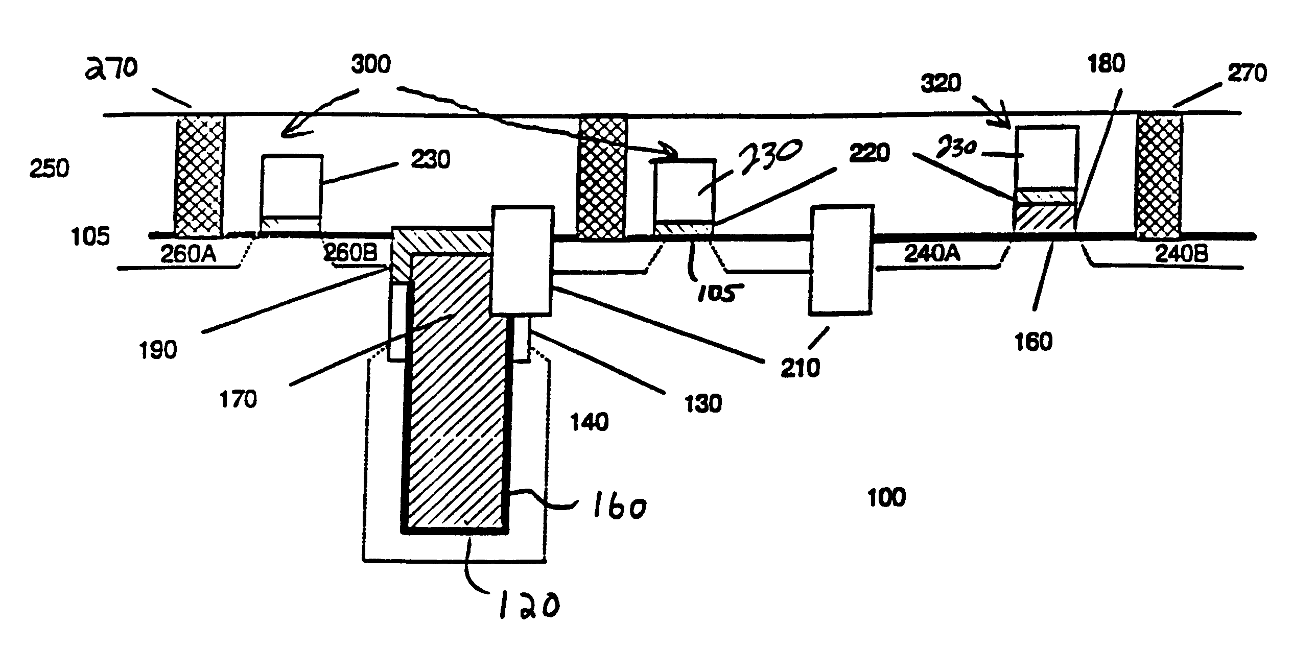
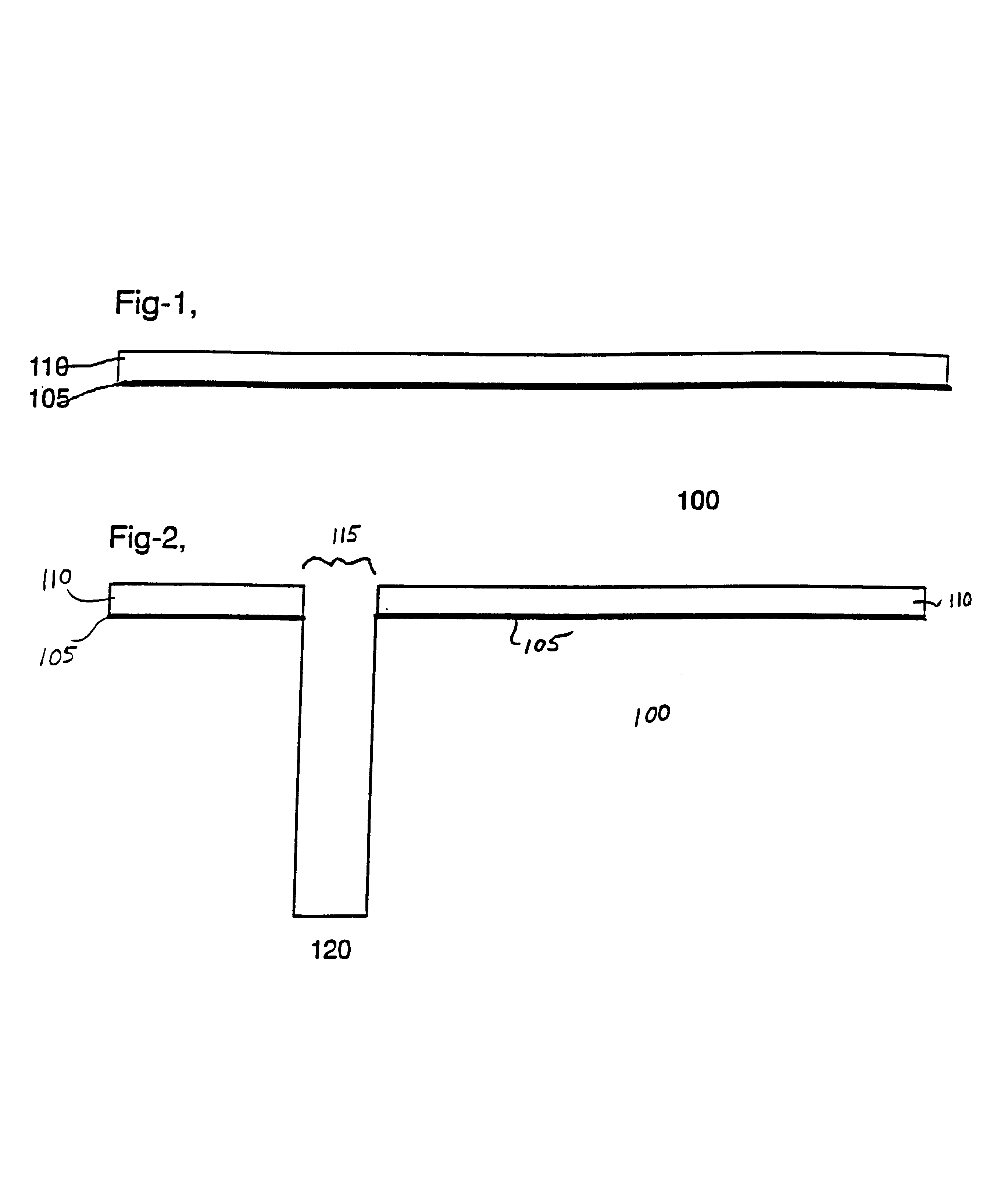
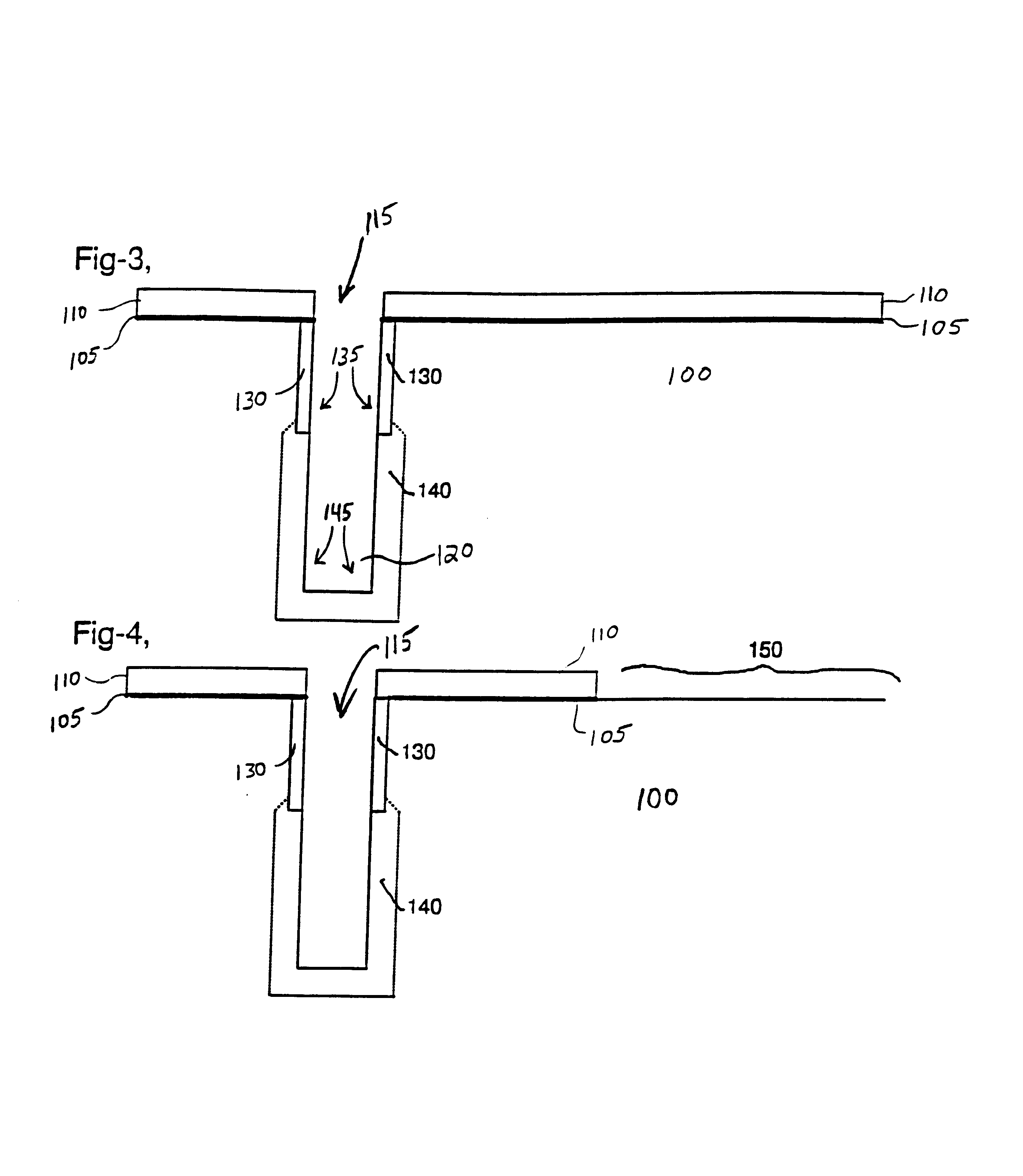
As mentioned above, there is a need to reduce the cost and improve performance of DRAM. The invention addresses these needs by providing a single high-k material for both device gate dielectrics as well as capacitor dielectrics in a DRAM device. In a preferred embodiment the invention uses a high-k film made using atomic level chemical vapor deposition (ALCVD) techniques. Using ALCVD to deposit a combination of La.sub.2 O.sub.3 / Al.sub.2 O.sub.3 obtains a dielectric constant between 10 and 30 depending on the ratio of Al to La. The invention uses deposition conditions that retain the amorphous nature of the film stack in order to prevent electrical leakage.

A new cell structure is proposed to form such a dielectric for both support gates and capacitor devices in one process step so as to significantly reduce the process cost. The high-k dielectric will not only improve the support device performance but will also boost the charge storage capability of the DRAM cells.

The high-k dielec...


PUM


Abstract

A method and structure for an improved DRAM (dynamic random access memory) dielectric structure, whereby a new high-k material is implemented for both the support devices used as the gate dielectric as well as the capacitor dielectric. The method forms both deep isolated trench regions used for capacitor devices, and shallow isolated trench regions for support devices. The method also forms two different insulator layers, where one insulator layer with a uniform high-k dielectric constant is used for the deep trench regions and the support regions. The other insulator layer is used in the array regions in between the shallow trench regions.

Description

1. Field of the InventionThe present invention generally relates to integrated storage devices and more particularly to an improved dynamic random access memory dielectric structure, and the method for producing the same.2. Description of the Related ArtDRAM, the dynamic random access memory, is known to have a much higher memory density than the SRAM, or the static random access memory. Usually, in order to achieve a high integration density, either a deep trench-capacitor or a high-k dielectric stack-capacitor cell is employed. Although the deep trench capacitor has a planar surface topography, the depth of the trench has become the limiting factor in preventing the scaling of DRAM exceeding 4 gigabytes. However, the high-k dielectric stack-capacitor cell is limited by the material stability as well as the topography. Here, the stack-capacitor is built on top of the silicon surface. Thus, the resulting non-planar surface has created problems for metallization as well as lithograph...

Claims


Application Information

Patent Timeline
Patent Type & Authority Patents(United States)
IPC IPC(8): H01L21/70H01L29/66H01L21/8242H01L31/0328H01L31/0264H01L29/94H01L21/28H01L21/316H01L21/334H01L27/108H01L29/51
CPCH01L21/28194H01L29/945H01L29/517H01L29/66181H01L21/31604H01L21/3162H01L27/1087H01L27/10829H01L21/02178H01L21/0228H10B12/37H10B12/0387
Inventor CLEVENGER, LAWRENCE A.HSU, LOUIS L.RADENS, CARL J.SHEPARD, JR., JOSEPH F.
Owner GLOBALFOUNDRIES INC
Why Eureka
Try Eureka