

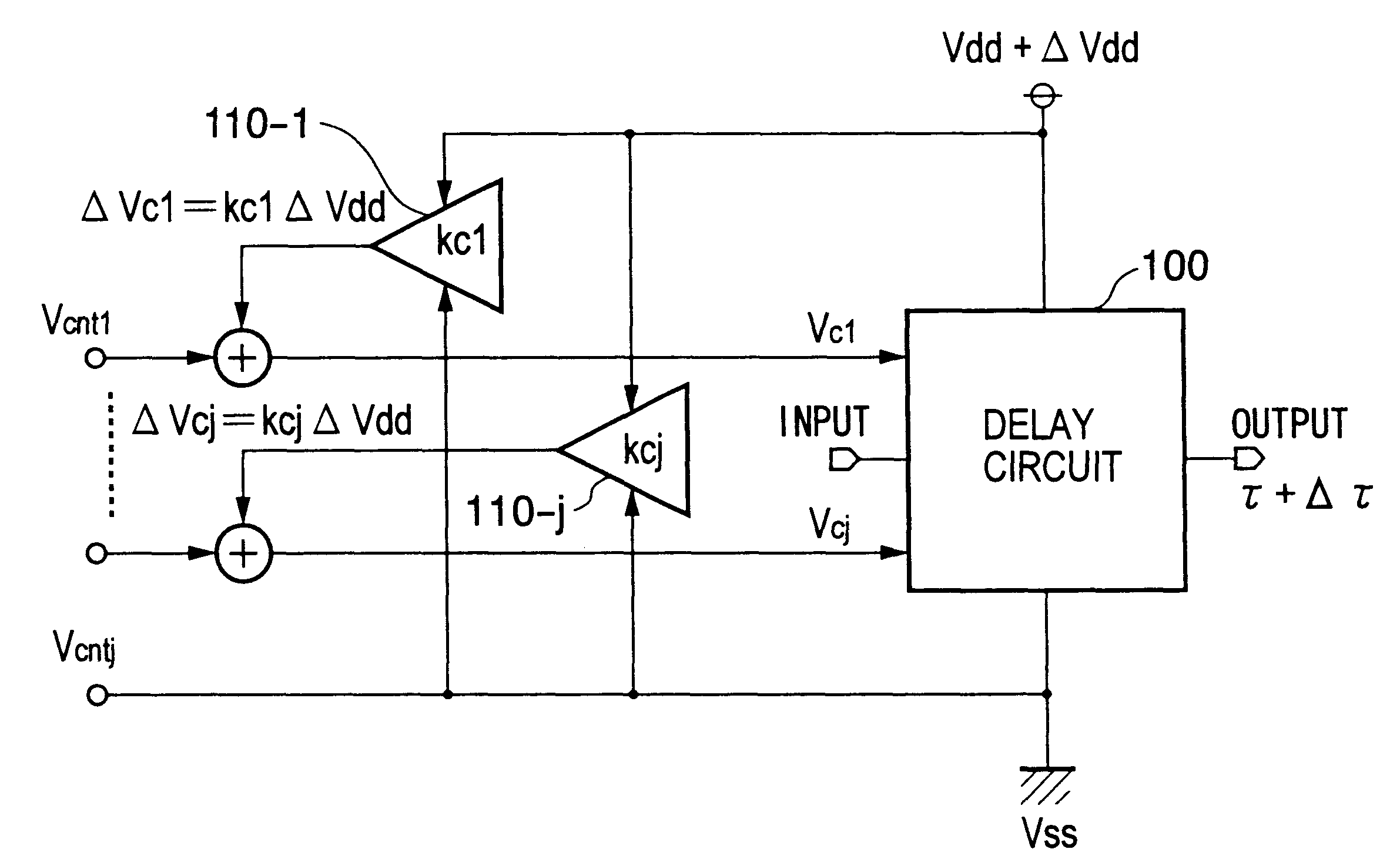
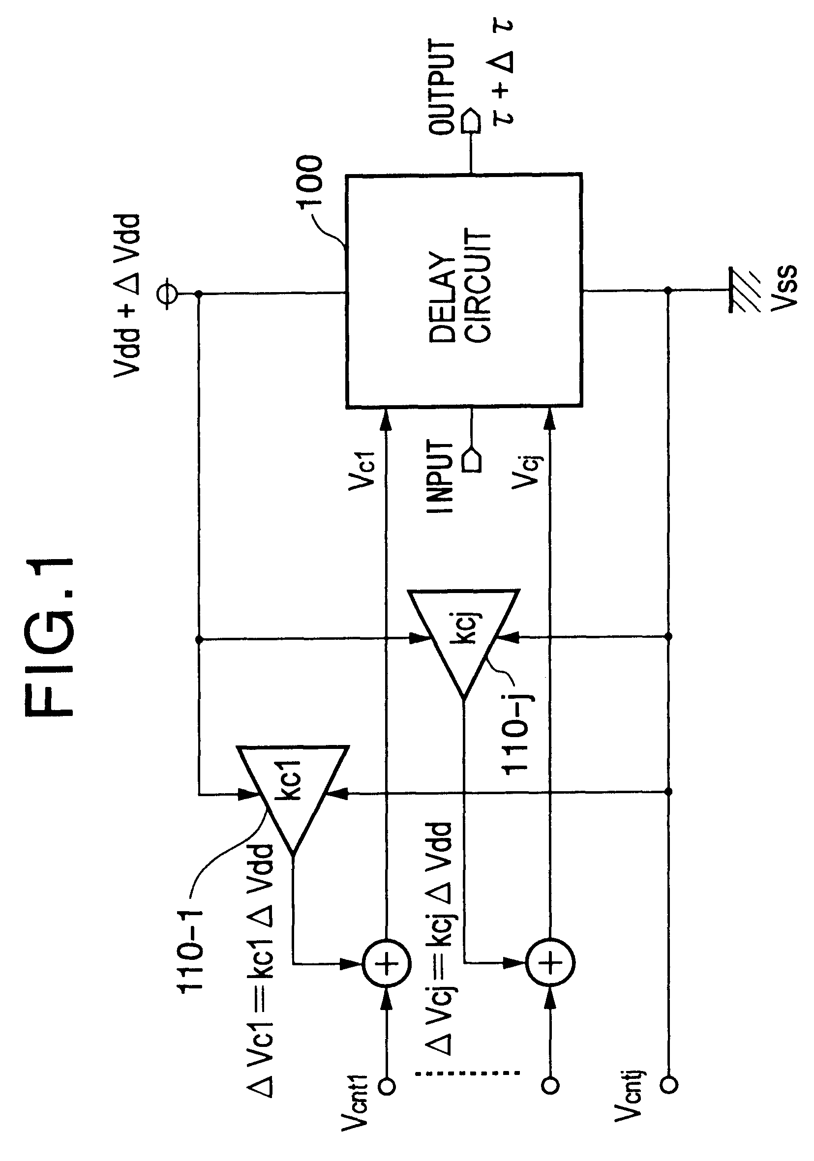
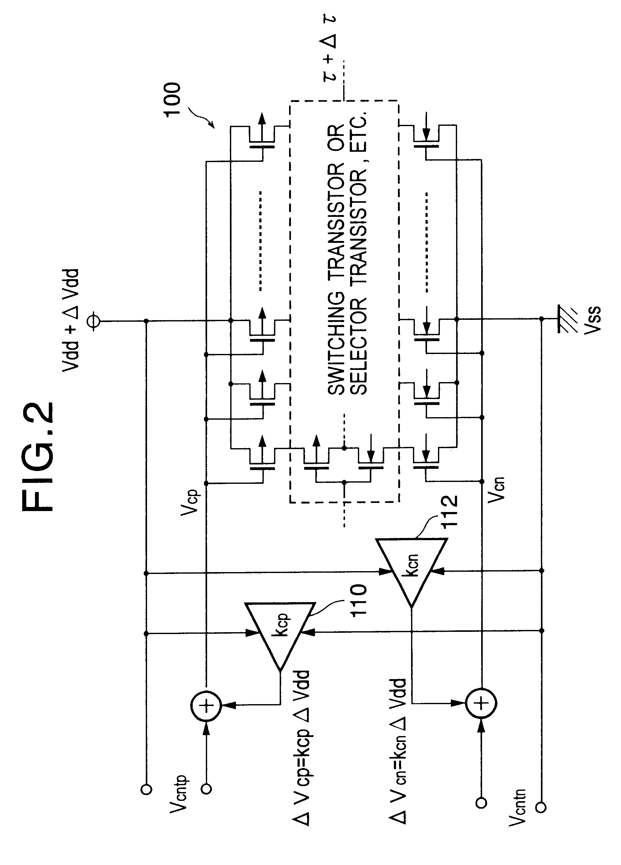
Delay circuit, voltage-controlled delay circuit, voltage-controlled oscillation circuit, delay adjustment circuit, DLL circuit, and PLL circuit
a delay circuit and voltage control technology, applied in the field of delay circuits, can solve the problems of increased susceptibility to process variations, reduced pull-in speed, and difficulty in designing a pll circuit of a very high multiplication factor
- Summary
- Abstract
- Description
- Claims
- Application Information
AI Technical Summary
Problems solved by technology
Method used
Image

Examples
second example
of Application
FIG. 41 is a circuit diagram of an example of application of the voltage-controlled oscillation circuit (VCO) of the present invention and shows a PLL circuit configured by using the VCO of the present example.
As shown in the figure, the PLL circuit of the present example is comprised of a phase comparator 10, a charge pump circuit 20, a filter 30, a VCO 40, and a frequency divider 50.
Note that, as shown in FIG. 41, the PLL circuit of the present example of application has almost the same configuration as a conventional PLL circuit. Note that even when the phase comparator 10, charge pump circuit 20, or the filter 30 is as same as a conventional type, it is possible to obtain an effect of remarkably reducing jitter caused by the power source voltage after pull-in by the PLL circuit by using the VCO of the present invention.
Note that since the effect of the present invention is obtained when a variety of conditions are attained well, the invention is not suited well for...
third example
of Application
FIG. 43 is a circuit diagram of a PLL circuit configured by using the VCO of the present invention and a dot clock generation circuit including this PLL circuit.
The dot clock generation circuit of the present example can be applied for example to a generation circuit for generating a dot clock and a VBI sampling clock for digital TV. The PLL circuit for example uses as a reference clock a horizontal synchronization signal HSYNC selected from a horizontal synchronization signal HSYNC0 of a main screen or a horizontal synchronization signal HSYNC1 of a sub-screen and synchronizes with a frequency divider output at a rising edge (corresponding to a right end of the screen) of the same. The charge pump circuit operates at the right end of the screen.
As shown in the figure, the PLL circuit portion is comprised of a phase comparator 10, charge pump 20, filter 30, VCO 40, frequency divider 50, and bias circuit 70. Other than the PLL circuit, a control circuit 400, a VBI sampl...
PUM
 Abstract
Description
Claims
Application Information