Method for in situ removal of a dielectric antireflective coating during a gate etch process

a dielectric anti-reflective coating and gate etching technology, which is applied in the direction of basic electric elements, electrical equipment, semiconductor devices, etc., can solve the problems of increasing the etch rate of the darc layer, affecting the performance of the device, and ultimately within the device,

Inactive Publication Date: 2003-09-02
APPLIED MATERIALS INC
View PDF19 Cites 26 Cited by
  • Summary
  • Abstract
  • Description
  • Claims
  • Application Information

AI Technical Summary

Problems solved by technology

However, despite the advantages of ARC usage described above, when an ARC layer (such as silicon oxynitride) acts as a dielectric, residual ARC layer presence in an etched film stack (and ultimately within the device) may affect the performance of the device.
Th

Method used


Image

  • Method for in situ removal of a dielectric antireflective coating during a gate etch process
  • Method for in situ removal of a dielectric antireflective coating during a gate etch process
  • Method for in situ removal of a dielectric antireflective coating during a gate etch process

Examples


example one

In this set of experiments, a silicon oxynitride DARC layer was etched simultaneously during a polycide gate etch process. FIG. 3 shows the various layers of the particular film stack used in this set of experiments. The film stack 301 included, from top to bottom, a silicon oxynitride layer 313, having a thickness of about 800 .ANG.; a "TEOS" (tetraethyl orthosilicate) deposited silicon oxide layer 311, having a thickness of about 1300 .ANG.; a tungsten silicide layer 309, having a thickness of about 800 .ANG.; a doped polysilicon layer 307, having a thickness of about 1500 .ANG.; and a gate oxide layer 305, having a thickness of about 70 .ANG., all deposited on a single-crystal silicon substrate 303. The film stack 301 was patterned using a conventional photoresist, which was removed prior to etching the silicon oxynitride and tungsten silicide layers. The TEOS-deposited silicon oxide layer 311 has been partially etched away in steps preceding the removal of the photoresist. FIG. ...

example two

In this experiment, residual silicon oxynitride DARC layer was removed simultaneously during etching of a doped polysilicon gate. FIG. 4 shows the various layers of the particular film stack used in this set of experiments. The film stack 401 included, from top to bottom, a silicon oxynitride layer 411, having a thickness of about 570 .ANG.; a TEOS deposited silicon oxide layer 409, having a thickness of about 500 .ANG.; a doped polysilicon layer 407, having a thickness of about 2000 .ANG.; and a gate oxide layer 405, having a thickness of about 52 .ANG., all deposited on a single-crystal silicon substrate 403. The film stack 401 was patterned using a conventional photoresist, which was removed prior to etching the silicon oxynitride and doped polysilicon layers. The TEOS-deposited silicon oxide layer 407 has been partially etched away in steps preceding the removal of the photoresist. FIG. 4 also shows the silicon oxynitride layer 409 partially removed.

One wafer having the structur...

example three

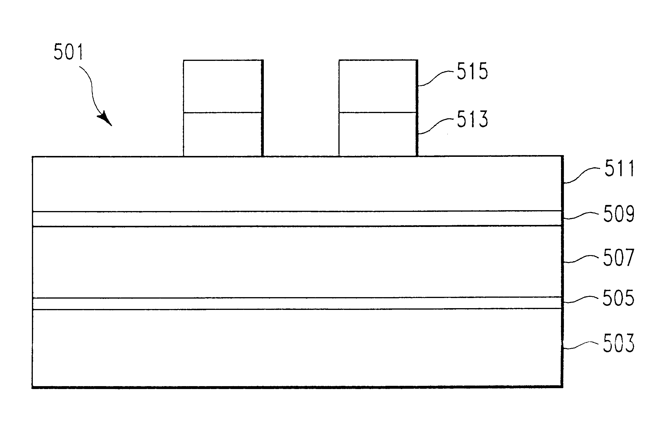
The method of the present invention could also be used for the simultaneous removal of a DARC layer during a tungsten metal gate etch process. FIG. 5 illustrates a typical film stack including a tungsten metal layer. The film stack 501 includes, from top to bottom, a silicon oxynitride layer 515, having a thickness of about 1100 .ANG.; a TEOS deposited silicon oxide layer 513, having a thickness of about 1000 .ANG.; a tungsten layer 511, having a thickness of about 1000 .ANG.; a titanium nitride barrier layer 509, having a thickness of about 300 A; an N+ and P+ doped polysilicon layer 507, having a thickness of about 1500 .ANG.; and a gate oxide layer 505, having a thickness of about 70 .ANG., all deposited on a single-crystal silicon substrate 503. The film stack 501 is typically patterned using a conventional photoresist, which is removed prior to etching the silicon oxynitride and tungsten layers. The TEOS-deposited silicon oxide layer 513 is partially etched away in steps preced...


PUM


Abstract

The present invention provides a method for the simultaneous removal of an oxygen and/or nitrogen-containing dielectric antireflective coating ("DARC") during plasma etching of an underlying layer in a film stack. According to the method of the invention, the film stack is etched using a plasma containing reactive fluorine species. The concentration of reactive fluorine species within the plasma is controlled based on one or more of the following factors: the oxygen content of the antireflective coating, the nitrogen content of the antireflective coating, the thickness of the antireflection coating layer, and the thickness of the underlying film stack layer. The disclosure of the invention provides preferred combinations of plasma source gases which provide for the simultaneous removal of an oxygen and/or nitrogen-containing DARC layer during etching of an underlying etch stack layer, where the underlying stack layer comprises a metal silicide, polysilicon, or a metal. Also provided herein is a formula for determining the total amount of DARC removed using a given etch process recipe, based on the etch selectivity of the particular process recipe

Description

1. Field of the InventionThe present invention pertains to a method for the simultaneous removal of an oxygen and / or nitrogen-containing dielectric antireflective coating ("DARC") during plasma etching of an underlying layer in a film stack.2. Brief Description of the Background ArtIn the field of semiconductor device fabrication, photoresists have been developed which are responsive to shorter wavelengths within the electromagnetic spectrum to enable the patterning of small-dimensioned electronic and optical devices. An example of one such class of photoresists are the deep ultraviolet photoresists ("DUV"), which are responsive to the shorter wavelengths in the ultraviolet region of the electromagnetic spectrum to pattern small dimensioned electronic and optical devices. The dimensions patterned with DUV photoresist are significantly smaller than device dimensions patterned using traditional or I-line photoresists.Generally, a photoresist is used to provide a pattern on the surface...

Claims


Application Information

Patent Timeline
IPC IPC(8): H01L21/02H01L21/027H01L21/3213H01L21/28H01L21/311
CPCH01L21/0276H01L21/32136H01L21/32139H01L21/28123H01L21/31116H01L21/32137H01L21/3065
Inventor JAIN, MOHITLILL, THORSTENCHINN, JEFF
Owner APPLIED MATERIALS INC
Why Eureka
Try Eureka