Silicon carbide power devices having increased voltage blocking capabilities

a technology of silicon carbide and power device, which is applied in the direction of semiconductor/solid-state device manufacturing, semiconductor devices, electrical apparatus, etc., can solve the problems of the thickness of the drift region, the limited maximum switching frequency achievable using conventional thyristors, and the inherent performance limitations of silicon thyristors

Inactive Publication Date: 2004-05-11
UNITED STATES OF AMERICA THE AS REPRESENTED BY THE SEC OF THE ARMY
View PDF13 Cites 27 Cited by
  • Summary
  • Abstract
  • Description
  • Claims
  • Application Information

AI Technical Summary

Benefits of technology

The embodiments of the invention achieve several advantages. For example, the invention reduces the number of processing steps involved in forming a high voltage blocking device because the lithography and deposition steps needed for field rings and field plates, or the lithography, implant and annealing processing steps required of guard rings or junction termination extensions can be avoided. An embodiment of the invention also makes it possible to develop high voltage blocking devices by using a thinner overall drift region which has the added benefit of lower cost and better material quality. In fact, because the material quality worsens as an epilayer becomes thicker, which is a problem inherent in the conventional devices, an embodiment of the invention overcomes this deficiency by providing thinner multiple layers.

Problems solved by technology

Although V.sub.f determines the on-state power loss of the device at any given current, the switching power loss becomes a dominating factor affecting the device junction temperature at high operating frequencies.
Because of this, the maximum switching frequencies attainable using conventional thyristors are limited, as compared with many other types of power devices.
However, thyristors made of silicon have certain performance limitations inherent in the silicon material itself, such as the thickness of the drift region.
However, the conventional devices are limited by the inherent characteristics of the silicon semiconductor material itself.
This, in turn, requires that these portions be physically thicker, which makes for a generally disadvantageous specific resistance.
However, one major limitation to the use of conventional silicon carbide GTO thyristors in these systems is the low turn-off gain.
If the turn-off gain is low, then the switching losses will be high, thereby reducing the amount of power that a single silicon carbide GTO thyristor can handle.
Also, the circuit providing the gate drive current to turn off the GTO thyristor requires extremely robust devices, which increases the cost and complexity of the overall system.
Unfortunately, the conventional devices have not achieved the level of satisfaction sought.
However, the performance and yield in large batches of these conventional devices remain unacceptable.
Thus, the conventional devices are underachieving.
Furthermore, the thick material is difficult to grow, leading to rough surfaces and poor electrical characteristics such as low free carrier lifetimes and mobility (electron and hole mobilities).
Unfortunately, this brings the maximum value of the electrostatic field near the surface of mesa isolated devices.
This causes disadvantageous effects because physical corners, such as those between the mesa and the flat silicon carbide regions outside of the mesa, create mesa isolation, and further concentrate the electrostatic field, thereby increasing the carrier generation due to impact ionization.
Moreover, the conventional devices use oxides deposited on the surface of the devices, wherein these surfaces are very close to this high electrostatic field region, leading to additional breakdown.
Moreover, the multiple epilayers block voltages in the device.

Method used


Image

  • Silicon carbide power devices having increased voltage blocking capabilities
  • Silicon carbide power devices having increased voltage blocking capabilities
  • Silicon carbide power devices having increased voltage blocking capabilities

Examples


first embodiment

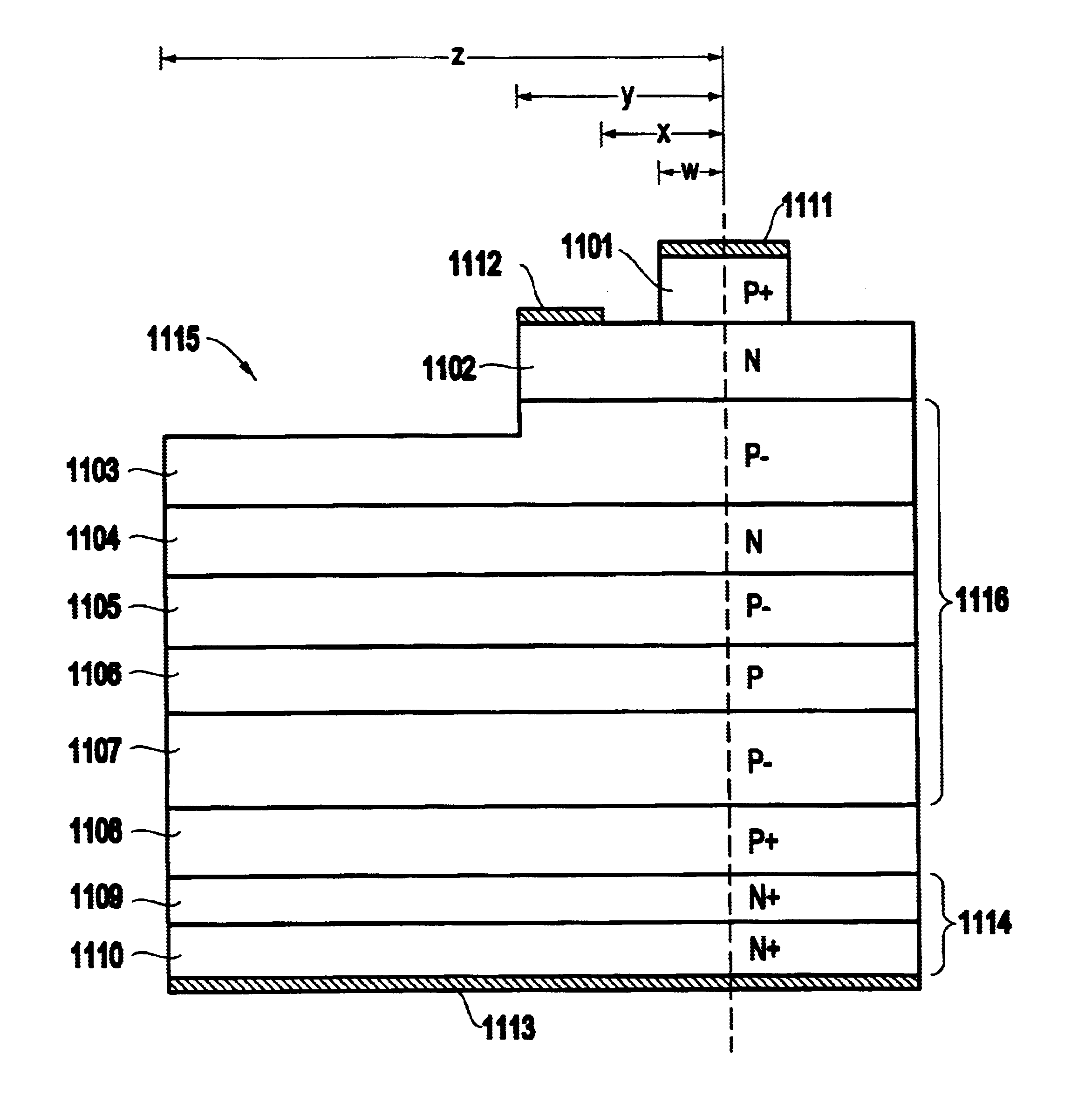
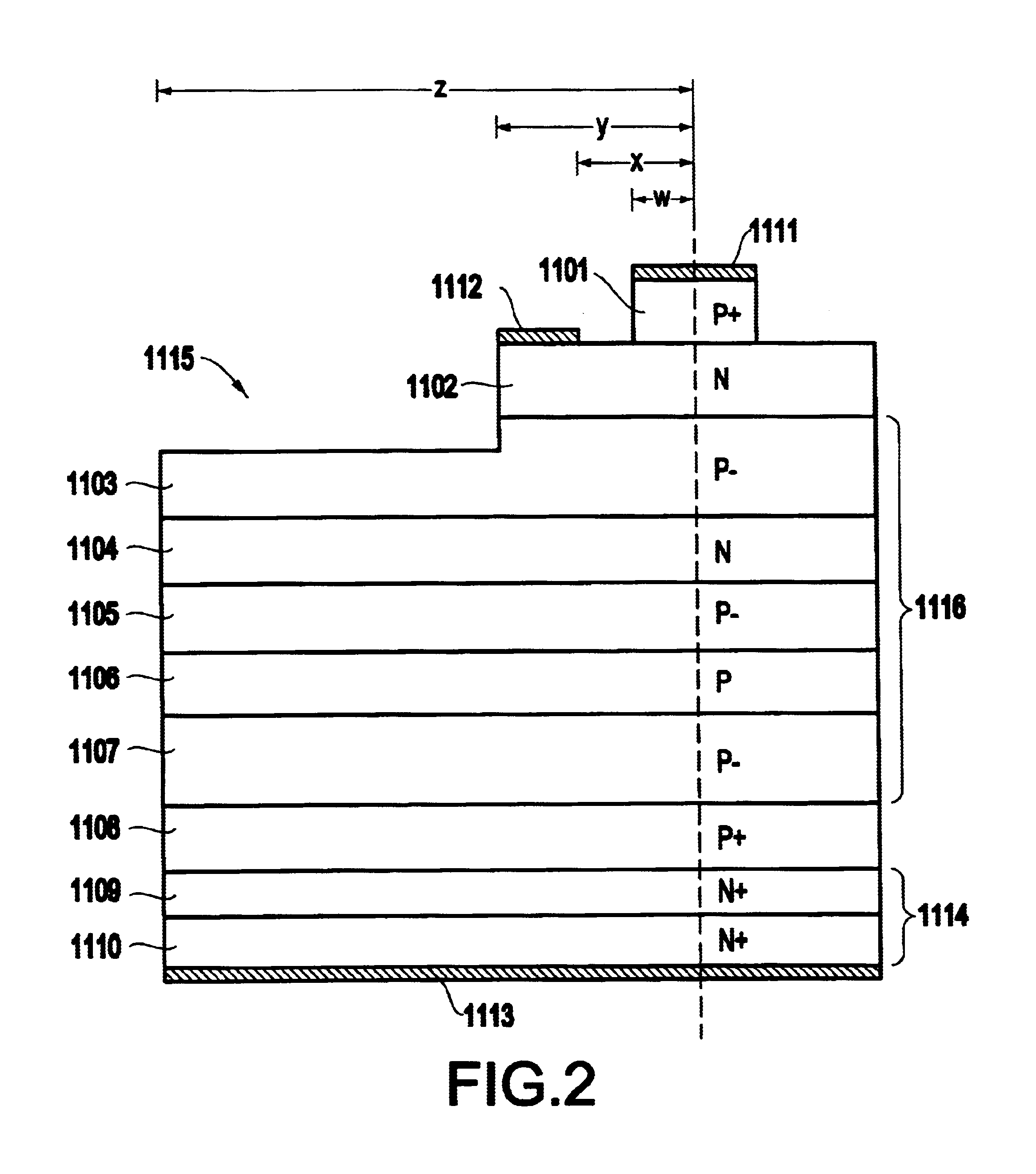
the invention is illustrated in FIG. 2, which provides a silicon carbide distributed buffer GTO thyristor 1115 comprising an anode 1101, a gate 1102 adjacent to the anode 1101, a multi-layered drift region 1116 (collectively comprising doped layers 1103, 1104, 1105, 1106, 1107) adjacent to the gate 1102, a high doped P+ buffer layer 1108 adjacent to the drift region 1116, a N+ layer 1109 adjacent to the P+ buffer layer 1108, and a substrate 1110 adjacent to the N+ layer 1109, wherein region 1109 and substrate 1110 collectively form the cathode region 1114 of the device 1115. The substrate 1110, the anode 1101, the drift region 1116, the gate 1102, and the cathode 1114 are each preferably formed of silicon carbide having a polytype comprising any of 3C, 2H, 4H, 6H, and 15R. The regions labeled p- or n- in FIG. 2 are the lowest doped semiconductor regions (the intrinsic or "i" regions). As an example, the device 1115 may be dimensioned to be 3.0 .mu.m as indicated by dimension w, 5.0 ...

fourth embodiment

the invention is shown in FIG. 5, where a thyristor device 200 is illustrated comprising a drift region 204 that includes a p-region 205, a new buffer n region 206, and an n-region 207. The epilayers 201 comprise the buffer region 203, the drift region 204, the gated base region 208, and the anode region 209. Gate contacts 211 and anode contacts 210 top the gated base region 208 and anode region 209, respectively. A substrate 202, which forms the cathode region 202, is also shown with a cathode contact 292 adjacent the cathode region 202. The regions labeled p- or n- in FIG. 5 are the lowest doped semiconductor regions (the intrinsic or "i" regions).

FIG. 6 illustrates a fifth embodiment of a thyristor device 300 according to the invention. The drift region 304 includes a n-region 305, a new buffer n region 306, a p-layer 307. The epilayers 301 comprise the buffer region 303, the drift region 304, the gated base region 308, and the anode region 309. Gate contacts 311 and anode contac...


PUM


Abstract

A structure and method for a voltage blocking device comprises a cathode region, a drift region positioned on the cathode region, a gate region positioned on the drift region, an anode region positioned on the gate region and a plurality of contacts positioned on each of the cathode region, the gate region, and the anode region, wherein the drift region comprises multiple epilayers having first doped type layers surrounding second doped type layers, wherein dopant concentrations of the first doped type layers are lower than dopant concentrations of the second doped type layers. The epilayers comprise at least one i-n-i layer and / or at least one i-p-i layer. Moreover, the multiple epilayers are operable to block voltages in the device.

Description

1. Field of the InventionThe present invention generally relates to semiconductor electronic switches, and more particularly to high power, high temperature gate-assisted turn-off thyristor devices, that use a multi-layered thick drift region to increase the voltage blocked.GOVERNMENT INTERESTThe invention described herein may be manufactured, used and / or licensed by or for the United States Government.2. Description of the Related ArtThyristors are bistable power semiconductor devices that can be switched from an off-stale to an on-state, or vice versa. Thyristors, along with other power semiconductor devices such as high-power bipolar junction transistors and power metal oxide semiconductor field effect transistors control or pass large amounts of current and block high voltages. Unlike conventional thyristors, a gate turn-off (GTO) thyristor is turned off by a reverse gate pulse. Generally, a trigger input implements conduction in GTO thyristors. Thereafter, the GTO thyristors be...

Claims


Application Information

Patent Timeline
Patent Type & Authority Patents(United States)
IPC IPC(8): H01L29/744H01L29/66H01L29/02H01L29/24
CPCH01L29/744H01L29/1608Y10S438/931Y10S257/918
Inventor SHAH, PANKAJ B.
Owner UNITED STATES OF AMERICA THE AS REPRESENTED BY THE SEC OF THE ARMY
Why Eureka
Try Eureka