Electronic device and its manufacturing method
a manufacturing method and technology for electronic devices, applied in semiconductor devices, semiconductor/solid-state device details, electrical apparatus, etc., can solve problems such as cracks or bulging in the molding itself, deterioration of the characteristics and reliability of the semiconductor device, and reducing the reliability of the electronic device entering the molding from external sources
- Summary
- Abstract
- Description
- Claims
- Application Information
AI Technical Summary
Benefits of technology
Problems solved by technology
Method used
Image

Examples
embodiment no.1
Embodiment No. 1
Now referring to FIG. 3(A), in the plasma process apparatus and CVD apparatus shown, the gas feeding system 5 is supplied with disilane (Si.sub.2 H.sub.6), through a line 17, ammonia, or nitrogen through a line 16, and argon 15, which is a non-product gas for the plasma process, through a line 15. These flows are controlled by a flowmeter 18 and a valves 19.
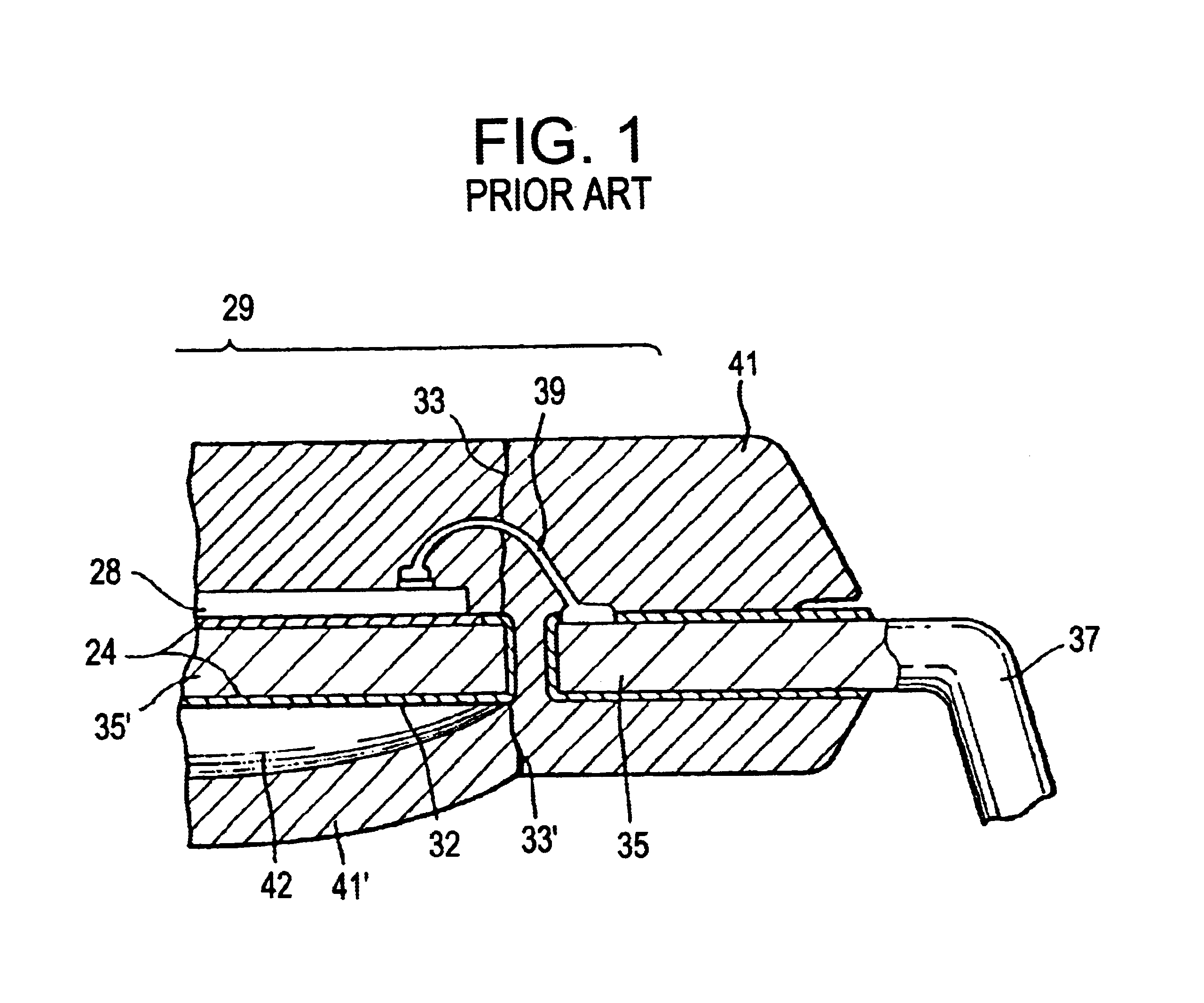
For example, the substrates 2 were maintained at room temperature (which includes self-heating as a result of the plasma), with heating from outside not being particularly actively carried out. Then, first, the substrates after molded, are placed in the reaction chamber 1. A vacuum of 1.times.10.sup.-3 Torr or less is drawn over the entire system for 10 to 30 minutes, so that the organic gases, chlorine, and moisture are removed from throughout the molding. After that, argon is introduced and the plasma process is carried out on the substrate 2, in particular on the surface of the molding 41. Specifically, the arg...
embodiment no.2
Embodiment No. 2
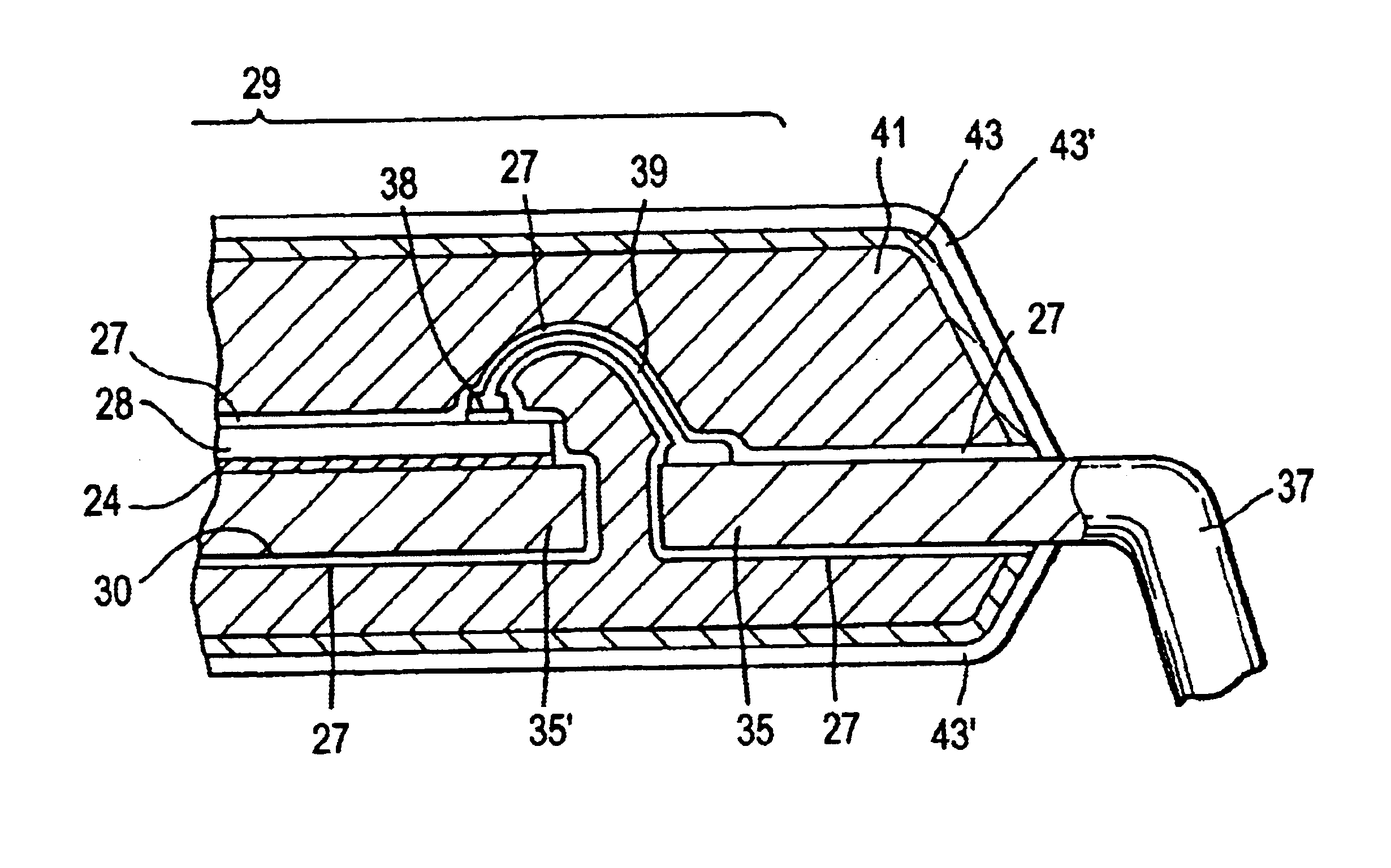
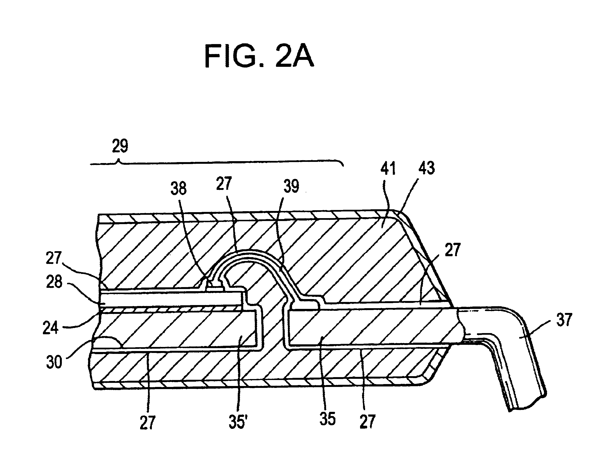
In this embodiment, an additional protective layer 43' shown in FIG. 2(B) wasformed on a substrate subjected to the same plasma process as in Embodiment No. 1. A silicon nitride film 43' was formed on a film-forming surface after the plasma process of Embodiment No. 1. The reactive gases used were NH.sub.3 / Si.sub.2 H.sub.6 / N.sub.2 in the ratio of 1 / 3 / 5. The electric energy was applied to these gases at an output of 1 kW at a frequency of 13.56 MHz for 10 to 30 minutes through the electrodes 11, 12. In this way a film was formed in about 30 minutes to an average thickness of 5000 .ANG..+-.200 .ANG.) at an average velocity of 3 .ANG. / sec.
The silicon nitride film had a dielectric strength of 8.times.10.sup.6 V / cm or greater and the specific resistance was 2.times.10.sup.15 .OMEGA.cm. The infrared absorption spectrum showed an Si-N bond absorption peak of 864 cm.sup.-1, and the refractive index was 2.0.
The electronic device manufactured in this manner was stored under ...
embodiment no.3
Embodiment No. 3
Now referring to FIG. 3(B), in the plasma CVD device shown, the gas feeding system 5 supplies a carbon fluoride, C.sub.2 F.sub.6 or C.sub.3 F.sub.8 through a line 20-1, a nitride gas, N(CH.sub.3).sub.3 through a line 20-3, ethylene through a line 20-2, hydrogen or argon, which is a non-product gas for the plasma process, through a line 20-15. These flows are controlled by a flowmeter 19 and a valve 18.
For example, the substrates 2 were maintained at room temperature (which includes self-heating as a result of the plasma), with heating from outside not being particularly actively carried out. Then, first, the substrate after molded, is placed in the reaction chamber 1. A vacuum of 1.times.10.sup.-3 Torr or less is drawn over the entire system for 10 to 30 minutes, so that the organic gases, chlorine, and moisture are removed from throughout the molding.
Then argon is introduced and an output of 1 kW at a frequency of 13.56 MHz is supplied to the pair of electrodes 11, ...
PUM
 Abstract
Description
Claims
Application Information
 - R&D
- Intellectual Property
- Life Sciences
- Materials
- Tech Scout
- Unparalleled Data Quality
- Higher Quality Content
- 60% Fewer Hallucinations
Browse by: Latest US Patents, China's latest patents, Technical Efficacy Thesaurus, Application Domain, Technology Topic, Popular Technical Reports.
© 2025 PatSnap. All rights reserved.Legal|Privacy policy|Modern Slavery Act Transparency Statement|Sitemap|About US| Contact US: help@patsnap.com