High throughput thin film deposition and substrate handling method and apparatus for optical disk processing

a technology of optical disk and substrate, applied in the field of high-throughput thin film deposition and substrate handling of optical disk substrate, can solve the problems of limiting the flexibility of cluster tools on the market, affecting the cost of manufacturing optical disks, and the optical disk industry struggling with system-related throughput problems. , to achieve the effect of convenient loading and unloading

Inactive Publication Date: 2004-07-27
PARK YOUNG
View PDF5 Cites 23 Cited by
  • Summary
  • Abstract
  • Description
  • Claims
  • Application Information

AI Technical Summary

Benefits of technology

In a second embodiment of the invention, shown in FIG. 6, there are two additional features for easy loading and unloading of a substrate 626 between the main and plenum chamber for loading 607 and plenum chamber for unloading 609. In particular, a central processing chamber 604 is maintained under vacuum, usually in the range of about 10.sup.-6 torr (1.3.times.10.sup.-4 Pa). The vacuum is maintained by a dedicated vacuum system (not shown) which is attached to vacuum ports 612A and 612B. This chamber is not exposed to air under normal deposition and substrate 626 loading and unloading steps. A plenum chamber for loading 607 is used to transfer a substrate 626 from a loading load-lock 608. Another plenum chamber for unloading 609 is used to transfer a substrate 626 from an unloading load-lock 610. Plenum chambers 607 and 609 are operated under a moderate vacuum, typically in the range of about 10.sup...

Problems solved by technology

Throughput or processing rate (number of substrates processed per hour) directly impacts on the cost of manufacturing the optical disks.
Due to the nature of the process steps used to produce an optical disk, and particularly thin film deposition where vacuum maintenance requirements and cleanliness (avoidance of substrate contamination by particulates) is critical in ensuring film quality, the optical disk industry has struggled with system-related throughput problems.
Despite these advantages, the types and capabilities of the component process modules/chambers and substrate transfer capabilities limit the flexibility of the cluster tools on the market.
One of the most significant detractors to cluster processing is mean time-to-failure (MTTF); this must be addressed with high priority, especially since an entire cluster is incapacitated when a single module fails.
The overall control of the multi-layer processing may be the most difficult aspect of the cluster system.
Due to an intrinsic nature of substrate routing sequence in a cluster tool system, the presently available software limits the maximum throughput.
Under this configuration, there are defects generated from the sputter target and shield areas, which affect on film quality and consequently product yield.
Use of pallets also increases the particle occurrence and overall cost of ownership (COO) from maintenance and spare stocks.
An in-line batch system may be able to handle up to about 100 substrates per hour for a single layer film deposi...

Method used


Image

  • High throughput thin film deposition and substrate handling method and apparatus for optical disk processing
  • High throughput thin film deposition and substrate handling method and apparatus for optical disk processing
  • High throughput thin film deposition and substrate handling method and apparatus for optical disk processing

Examples


Embodiment Construction

For purposes of this example, the optical recording medium comprises 4 layers of deposited thin films. In particular, the first deposited layer is a dielectric layer of SiO.sub.2 which is 80 nm thick. The second deposited layer is a recording layer of Ge.sub.3 Sb.sub.3 Te.sub.5 which is 20 nm thick. The third deposited layer is another dielectric layer of SiO.sub.2 which is 25 nm thick. The fourth deposited layer is a reflection layer of an aluminum alloy which is 60 nm thick. The first deposited layer is deposited on a substrate which is typically polycarbonate and which is approximately 0.6 mm to about 1.2 mm thick, and which is in the shape of a disk having a diameter of 120 mm (4.7 inches).

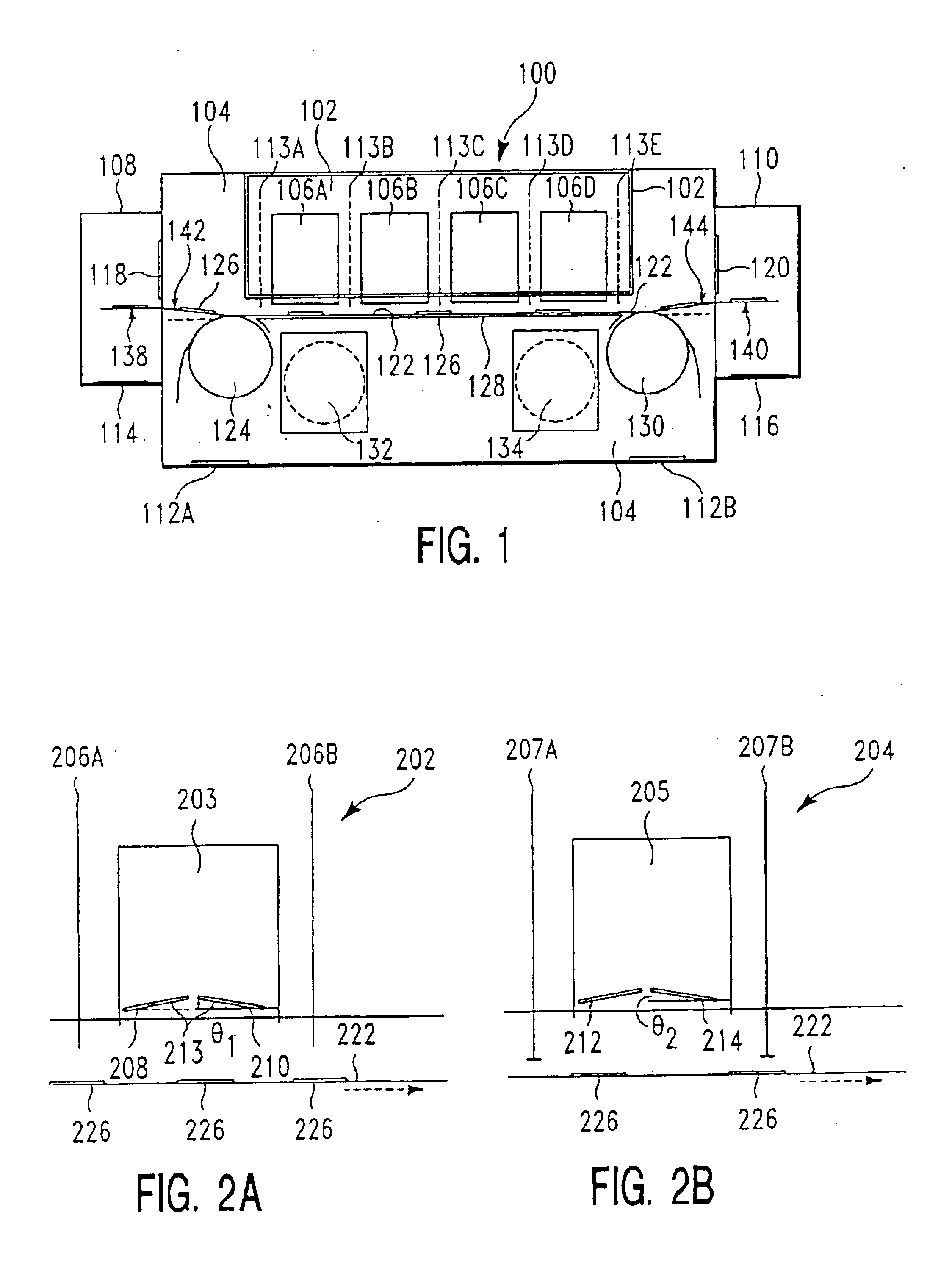
With reference to FIG. 1, the polycarbonate substrates are available from a cassette 138 of the kind known in the semiconductor industry for providing substrates. The cassette 138 is positioned in a loading chamber 108. Loading chamber 108 is held under vacuum at a pressure of about 10.sup.-4 ...


PUM

PropertyMeasurementUnit
Pressureaaaaaaaaaa
Poweraaaaaaaaaa
Transmissionaaaaaaaaaa

Abstract

The disclosure herein relates to a high throughput system for thin film deposition on substrates which can be used in applications such as optical disks, and in particular DVD disks, chip-scale packaging, and plastic based display, for example. An apparatus useful in the production of products of the kind described above includes: (a) a continuously moving web for simultaneously transporting a number of substrates to which a thin film of material is to be applied, wherein the moving web is a roll-to-roll moving web; (b) a central processing chamber which is maintained under vacuum and through which at least a portion of said continuously moving web travels; and, (c) at least one deposition device which is located within said central processing chamber, where at least a portion of said continuously moving web is exposed to material deposited from said deposition device. Typically the deposition device is a magnetron sputtering device. In addition, the apparatus typically also includes (d) a first moving platform which transfers a substrate onto said continuously moving web, and (e) a second moving platform which receives processed substrates from said continuously moving web.

Description

1. Field of the InventionThe present invention relates to a method and apparatus for high throughput thin film deposition upon and substrate handling of optical disk substrates. In particular, multi-layer thin films are deposited on substrates which are subsequently finished for use in optical disk applications such as DVD (digital versatile disk). To obtain increased processing efficiencies, the deposition apparatus includes a moving web which holds substrates in position as they are carried from one processing location to another.2. Brief Description of Background ArtThroughput or processing rate (number of substrates processed per hour) directly impacts on the cost of manufacturing the optical disks. Due to the nature of the process steps used to produce an optical disk, and particularly thin film deposition where vacuum maintenance requirements and cleanliness (avoidance of substrate contamination by particulates) is critical in ensuring film quality, the optical disk industry h...

Claims


Application Information

Patent Timeline
IPC IPC(8): C23C14/56
CPCC23C14/568
Inventor PARK, YOUNG
Owner PARK YOUNG
Why Eureka
Try Eureka