Method and apparatus for producing large, single-crystals of aluminum nitride

a technology of aluminum nitride and single crystals, which is applied in the direction of crystal growth process, polycrystalline material growth, chemically reactive gas, etc., can solve the problems of gan epitaxy cracking, gan epitaxy cracking during the cooling process after the device fabrication process, and high production cos

Inactive Publication Date: 2004-08-03
CRYSTAL
View PDF9 Cites 82 Cited by
  • Summary
  • Abstract
  • Description
  • Claims
  • Application Information

AI Technical Summary

Problems solved by technology

However, sapphire is far from being an ideal substrate for GaN epitaxy.
Its lattice mismatch to GaN is large (about 16%), it has little distinction between the + and - directions which can give rise to + / -c-axis domains in epitaxial films of GaN, and its differential thermal expansion can lead to cracking during the cooling process after the device fabrication process.
Using sapphire substrates leads to a costly fabrication process since it requires growing buffer layers and using Lateral Epitaxial Overgrowth techniques (LEO).
Even though this announcement is very promising, Nichia's lasers still have problems.
Sapphire, with a very low thermal conductivity, traps that heat, a fault that may trigger burnout down the road.
However, this alternative may increase fabrication cost.
However, 2H SiC (to match the 2H crystal structure of GaN) is not available and the lattice mismatch along the c-axis between GaN and both 4H and 6H SiC is substantial.
In addition, the chemical bonding between the Group IV elements of the SiC and the Group-III or Group-V elements of the nitrides is expected to create potential nucleation problems leading to electronic states at the interface.
While this possibility has become more attractive in the last few years, it does not appear to be commercially feasible to fabricate large bulk crystals of GaN in the short term.
Unfortunately, however, most attempts at increasing the growth rate of AlN crystals under such stoichiometric and / or sub atmospheric pressure conditions have met with limited success.
In addition, it appears to be impossible to achieve the growth rate, or the electronics-grade quality Hunter discloses in his patents with the nitrogen pressure below one atmosphere.
Disadvantageously, it would be difficult to grow large boules of AlN this way since: (i) control of growth would be difficult (since it would be non-uniform across the surface), (ii) a large amount of Al would be wasted, (iii) the excess Al in the rest of the furnace would create problems because of its high reactivity, and (iv) it would be difficult to maintain high differences in temperature (T) between the source and growing crystal surface.

Method used


Image

  • Method and apparatus for producing large, single-crystals of aluminum nitride
  • Method and apparatus for producing large, single-crystals of aluminum nitride
  • Method and apparatus for producing large, single-crystals of aluminum nitride

Examples


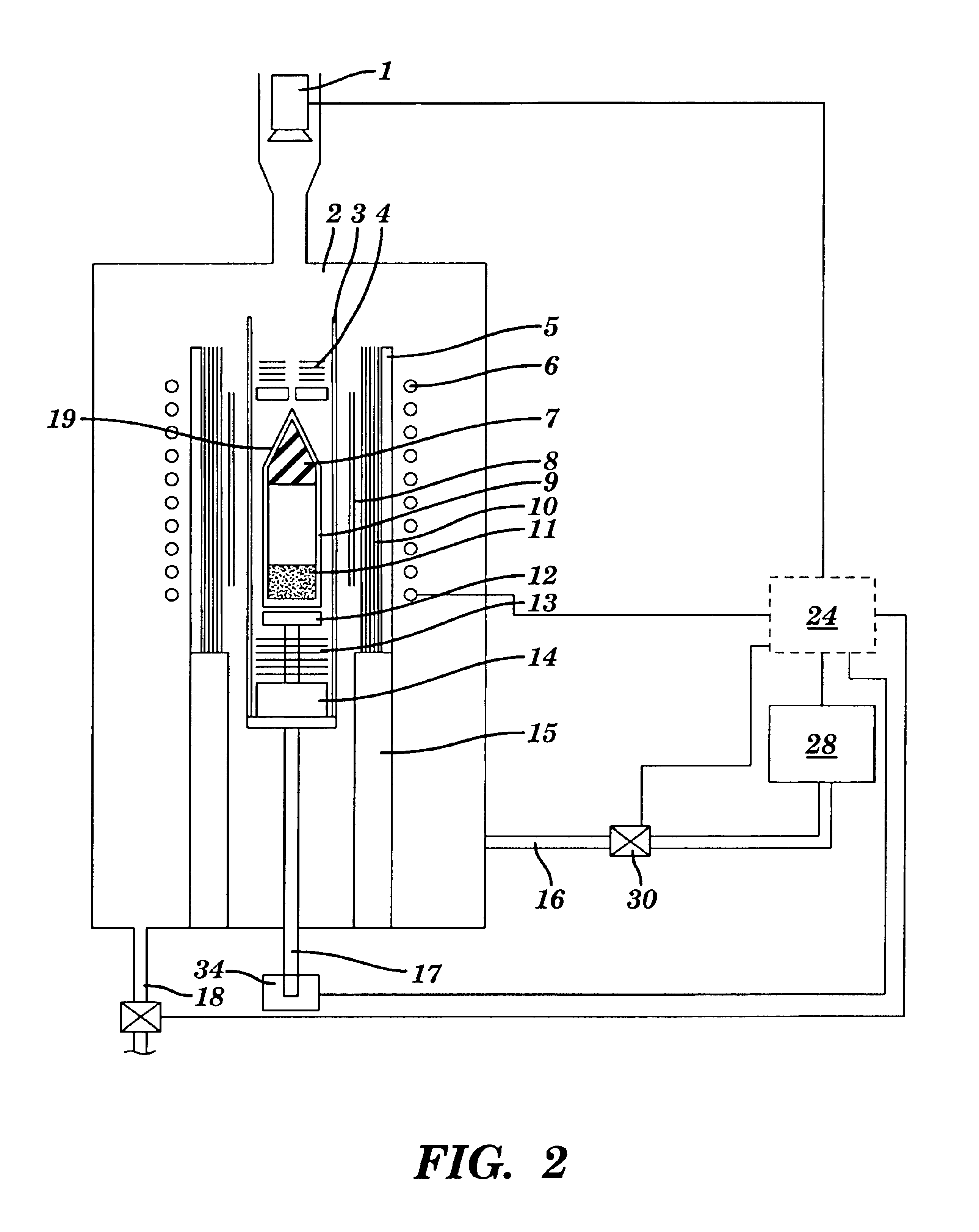
Embodiment Construction

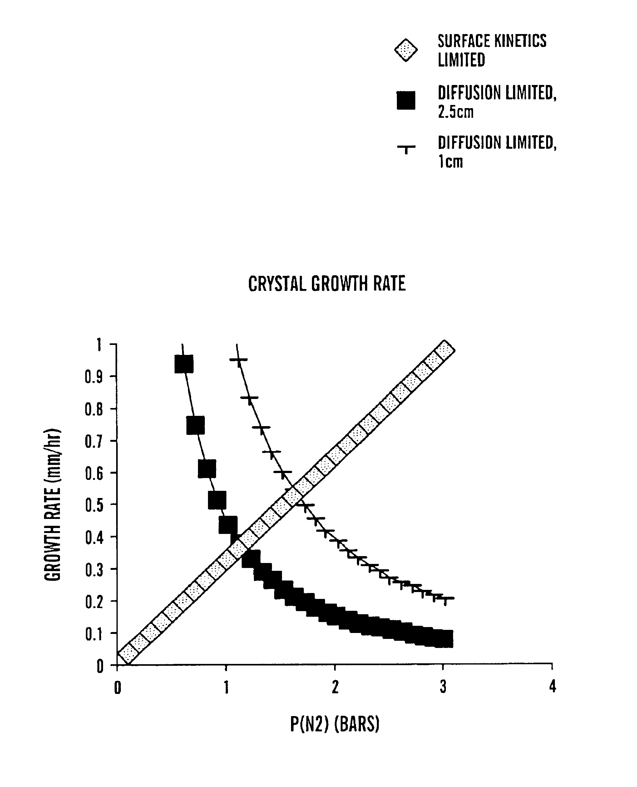
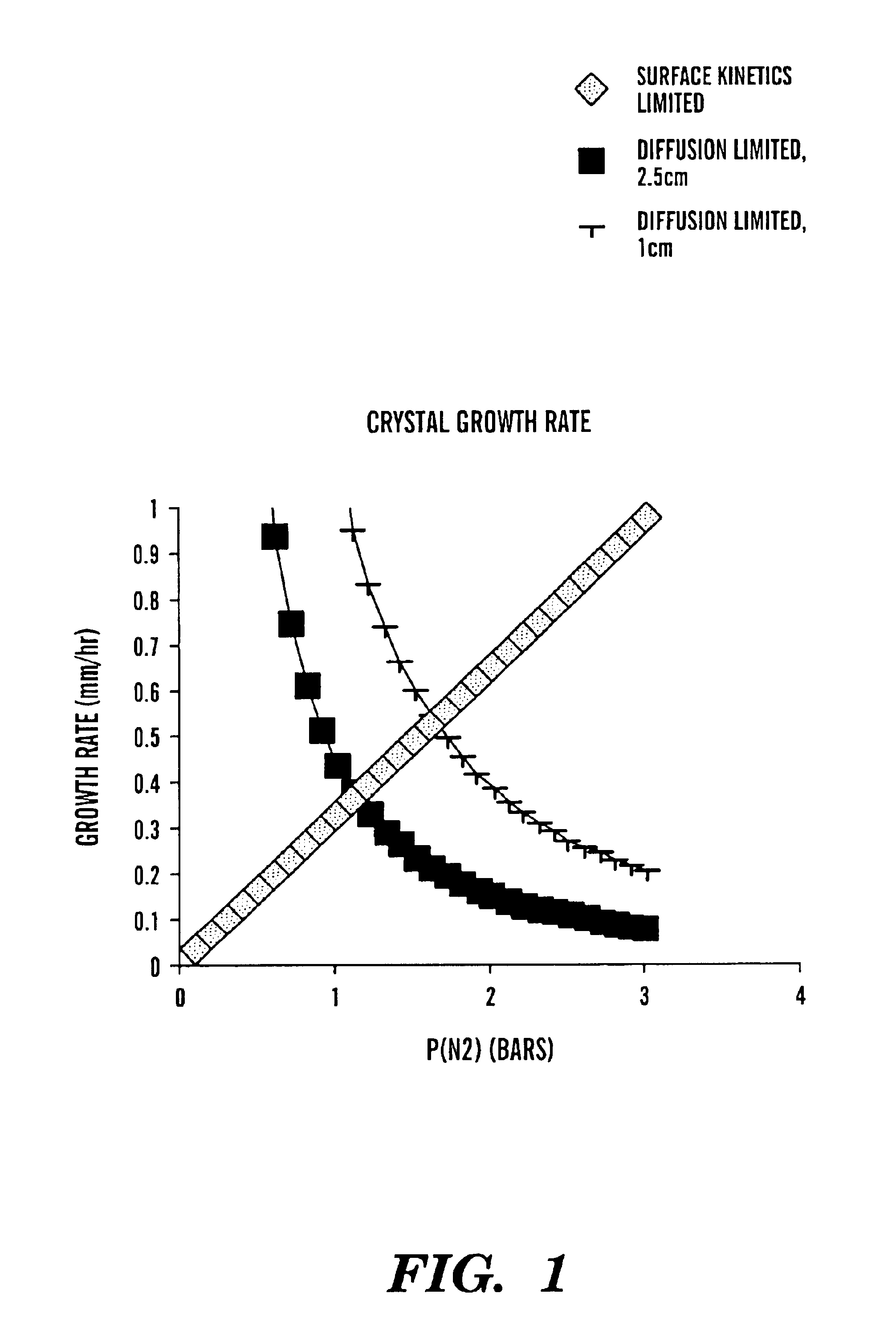
The present invention includes a method and apparatus for producing aluminum nitride (AlN) substrates that advantageously have a relatively small lattice mismatch (around 2.2%) with GaN, and have an almost identical thermal expansion from room temperature to 1000.degree. C. These AlN crystals also advantageously have the same wurtzite (2H) crystal structure as GaN and nominally the same type of piezoelectric polarity. Also, the chemical compatibility with GaN is much better than that of the SiC. In addition, AlN substrates tend to be attractive for Al.sub.x Ga.sub.1-x N devices requiring higher Al concentration (e.g., for high temperature, high power, radiation hardened, and ultra-violet (UV) wavelength applications).

Emerging optoelectronic and electronic devices based on the epitaxial growth of GaN and Al.sub.x Ga.sub.1-x N layers may significantly benefit from such an improved substrate. The size of the potential market, especially blue-violet light emitting diodes (LEDs) and lase...


PUM

PropertyMeasurementUnit
temperatureaaaaaaaaaa
pressureaaaaaaaaaa

Abstract

A method and apparatus for producing bulk single crystals of AlN includes a crystal growth enclosure with Al and N2 source material therein, capable of forming bulk crystals. The apparatus maintains the N2 partial pressure at greater than stoichiometric pressure relative to the Al within the crystal growth enclosure, while maintaining the total vapor pressure in the crystal growth enclosure at super-atmospheric pressure. At least one nucleation site is provided in the crystal growth enclosure, and provision is made for cooling the nucleation site relative to other locations in crystal growth enclosure. The Al and N2 vapor is then deposited to grow single crystalline AlN at the nucleation site.

Description

The present invention relates to the growth of single-crystal Aluminum Nitride (AlN), and more particularly, to relatively large, single-crystal AlN, which are grown by sublimation-recondensation at growth rates exceeding 0.5 mm / hr.BACKGROUND INFORMATIONStatus of III-Nitride Technology Using Commercially Available SubstratesSeveral types of materials are routinely used to form semiconductor substrates. Sapphire is popular, because relatively high-quality, inexpensive sapphire substrates are commercially available. However, sapphire is far from being an ideal substrate for GaN epitaxy. Its lattice mismatch to GaN is large (about 16%), it has little distinction between the + and -[0001] directions which can give rise to + / -c-axis domains in epitaxial films of GaN, and its differential thermal expansion can lead to cracking during the cooling process after the device fabrication process. In spite of those problems, recently, Nichia Ltd (Japan) has announced the production of the first ...

Claims


Application Information

Patent Timeline
Patent Type & Authority Patents(United States)
IPC IPC(8): C30B11/00C30B23/00
CPCC30B11/003C30B29/403C30B23/00Y10T117/10
Inventor SCHOWALTER, LEO J.SLACK, GLEN A.ROJO, J. CARLOS
Owner CRYSTAL
Why Eureka
Try Eureka