Light emitting device, method of manufacturing the same, and manufacturing apparatus therefor

a technology manufacturing method, which is applied in the direction of thermoelectric device, organic semiconductor device, discharge tube luminescnet screen, etc., can solve the problems of extremely high cost of circularly polarizing film, low film formation precision, and large size of light emitting devi

Inactive Publication Date: 2004-11-09
SEMICON ENERGY LAB CO LTD
View PDF5 Cites 99 Cited by
  • Summary
  • Abstract
  • Description
  • Claims
  • Application Information

AI Technical Summary

Benefits of technology

An object of the present invention is therefore to prevent turning the light emitting device into a mirrored surface without using a circularly polarizing film, and to provide a low cost light emitting device in which manufacturing costs for the light emitting device are thus lower. Low cost color filters are used by the present invention as a substitute for the circularly polarizing films. It is preferable to provide color filters in the light emitting device for each of the structures 1, 2, and 3 corresponding to each of the pixels in order to increase color purity. Furthermore, black color filter portions (black color organic resins) may also be formed overlapping the portions located between the light emitting regions. In addition, the black color filter portions may also overlap with the portions in which parts of different organic compound layers overlap with each other.
To solve this problem, the present invention employs a structure covered with a protective film made from a silicon nitride film or a silicon oxynitride film in which a silicon oxide film or a silicon oxynitride film is formed as a buffer layer in order to relieve stress in the protective film.
In addition, the aforementioned structure 4 is extremely useful for cases in which a transparent conductive film (typically ITO) is used as a cathode or an anode and a protective film is formed thereon. Note that, although there is a danger that impurities contained in the transparent conductive film (such as In, Sn, and Zn) will mix into a silicon nitride film contacting the transparent conductive film if the silicon nitride film is formed by sputtering, the impurities can be prevented from mixing into the silicon nitride film by forming the buffer layer of the present invention between the two films. The mixing in of impurities (such as In and Sn) form the transparent conductive film can be prevented by forming the buffer layer in accordance with the structure 4, and a superior protective film having no impurities can be formed.
Furthermore, the structure 4, in which the buffer layer and the protective film are formed, can be manufactured with good throughput by using the manufacturing apparatus shown in the structure 5.

Problems solved by technology

However, with these methods the film formation precision is not very high.
These demands become a big problem, however, in that the pitch between pixels becomes finer along with making the light emitting device higher in definition (increasing the number of pixels) and reducing the size of the light emitting device.
There is a problem with light emitting devices in that external light (light from outside of the light emitting device) made incident to pixels which are not emitting light is reflected by rear surfaces of the cathodes (surfaces contacting the light emitting layer), and the rear surfaces of the cathodes act as a mirror, reflecting external scenery in observation surfaces (surfaces toward an observer).
Further, although circularly polarizing films are bonded to the observation surfaces of the light emitting device in order to avoid this problem, the circularly polarizing films have an extremely high cost, and this is a problem in that it invites an increase in manufacturing costs.
Circularly polarizing films thus become unnecessary.
Further, the biggest problem in putting EL elements to practical use is that the element lifetime is insufficient.
Element degradation also becomes a large problem as EL layer degradation occurs with the appearance of dark spots spreading along with long time light emission.

Method used


Image

  • Light emitting device, method of manufacturing the same, and manufacturing apparatus therefor
  • Light emitting device, method of manufacturing the same, and manufacturing apparatus therefor
  • Light emitting device, method of manufacturing the same, and manufacturing apparatus therefor

Examples


embodiment mode 1

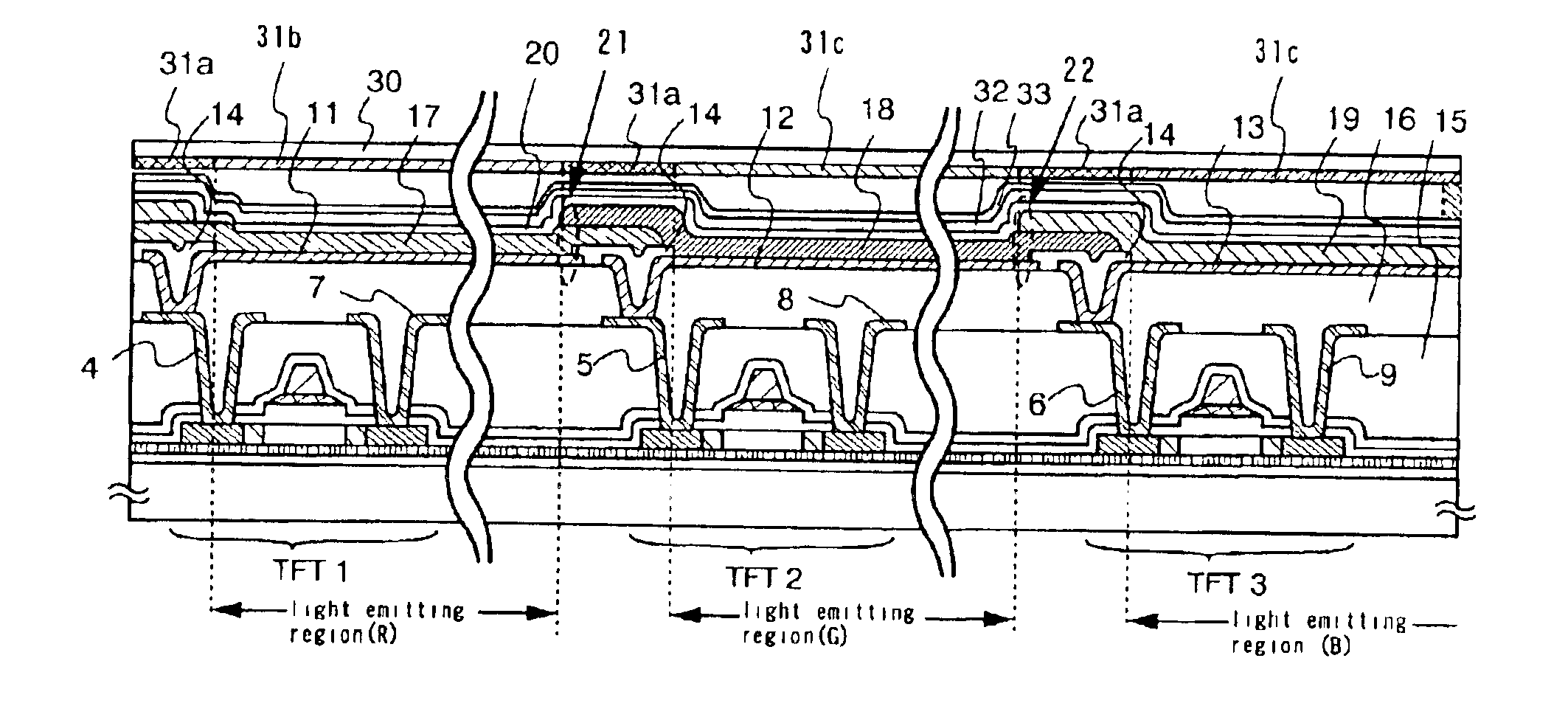
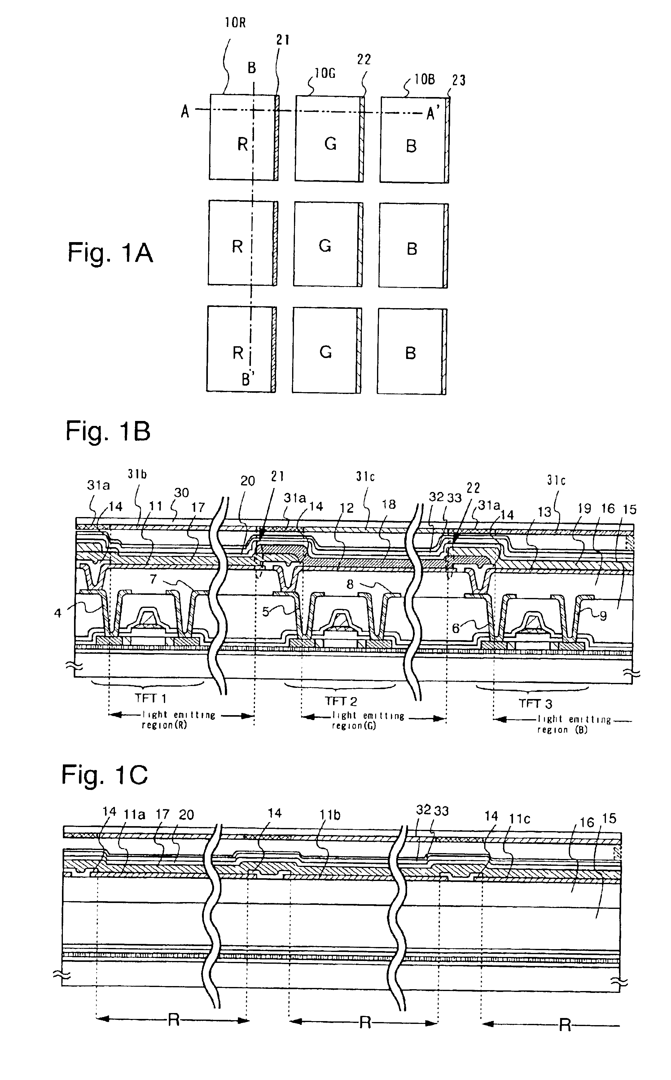
The present invention is explained below by an example of a 3.times.3 section of pixels from among many pixels disposed regularly in a pixel portion.

FIG. 1A is a top view. In FIG. 1A, a light emitting region 10R is a red color light emitting region, a light emitting region 10G is a green color light emitting region, and a light emitting region 10B is a blue color light emitting region. A full color light emitting device is achieved by the light emitting regions of the three colors.

Further, FIG. 1B is a cross sectional view of FIG. 1A sectioned along a dashed line segment A-A'. In the present invention, a portion of a red color light emitting EL layer 17 (for example, an EL layer in which Nile Red, a red color luminescent pigment is added to Alq.sub.3) overlaps with a portion of a green color light emitting element 18 (for example, an EL layer in which DMQd (dimethyl quinacridone) is added to Alq.sub.3), forming a laminate portion 21, as shown in FIG. 1B. Further, a portion of the gr...

embodiment mode 2

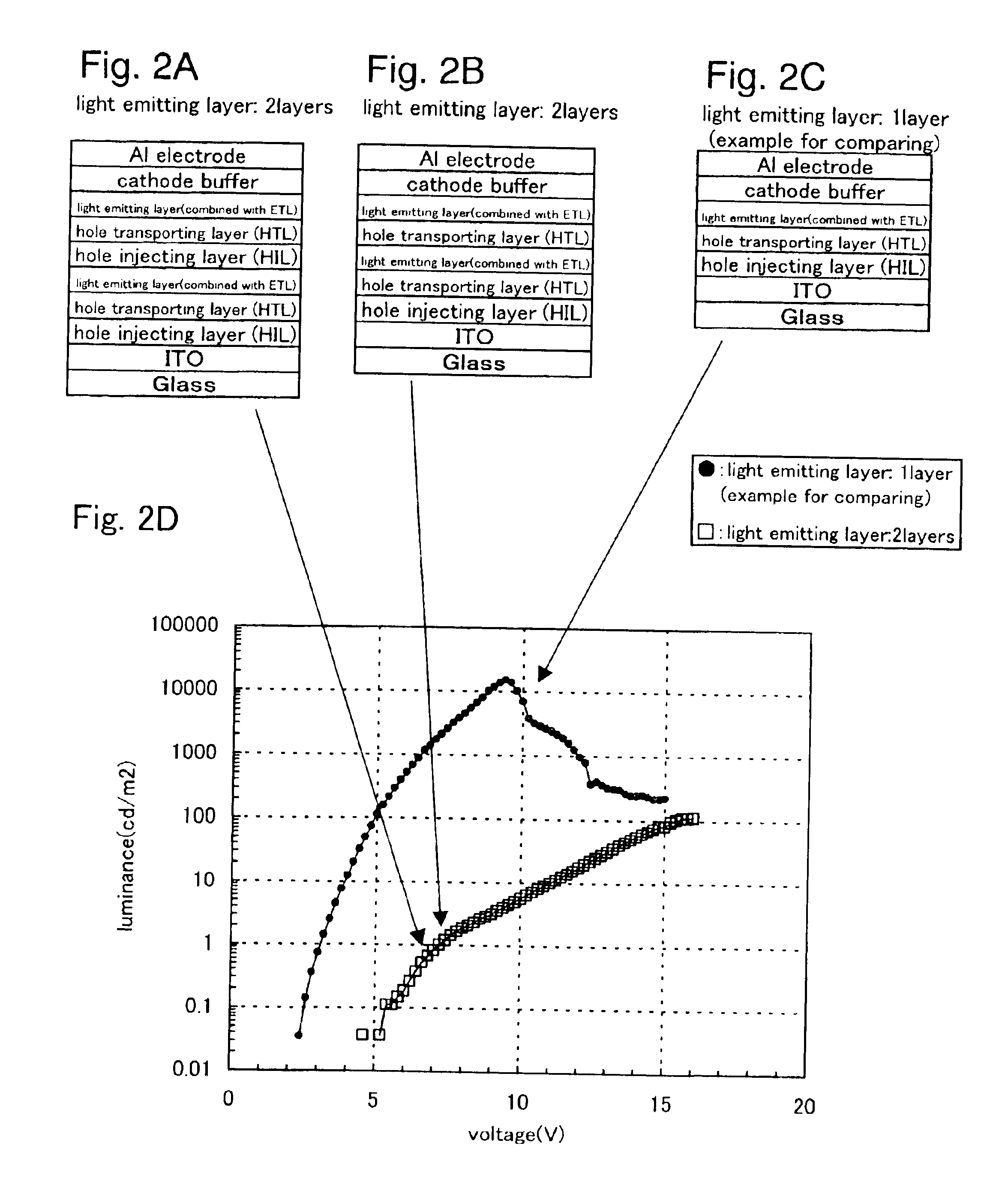
A buffer layer and a protective film are explained here using FIGS. 5A and 5B.

FIG. 5A is a schematic diagram showing an example of a laminate structure for a case in which light is emitted in the direction of an arrow within the figure. In FIG. 5A, reference numeral 200 denotes a cathode (or an anode), reference numeral 201 denotes an EL layer, reference numeral 202 denotes an anode (or a cathode), reference numeral 203 denotes a stress relieving layer (buffer layer), and reference numeral 204 denotes a protective film. A material having light transmitting characteristics, an extremely thin metallic film, or a laminate thereof is used as the electrode 202 when light is emitted in the direction of the arrow in FIG. 5A.

The protective film 204 uses an insulating film obtained by sputtering and having silicon nitride or silicon oxynitride as its main constituent. A silicon nitride film can be obtained provided that the protective film is formed using a silicon target under an atmosphere...

embodiment 1

In this embodiment, an active matrix type light emitting device manufactured on an insulating film will be described. FIG. 6 is a cross sectional view of the active matrix type light emitting device. As an active element, a thin film transistor (hereafter referred to as TFT) is used here, a MOS transistor may also be used.

A top gate TFT (specifically a planar TFT) is shown as an example, a bottom gate TFT (typically inversely staggered TFT) may also be used.

In this embodiment, a substrate 800 is used, which is made of barium borosilicate glass or alumino borosilicate glass, a quartz substrate, a silicon substrate, a metal substrate, or stainless substrate forming an insulating film on the surface may be used. A plastic substrate having heat resistance enduring a treatment temperature of this embodiment also may be used, and further a flexible substrate may be used.

Next, a silicon oxynitride film is formed as a lower layer 801 of a base insulating film on a heat-resistant glass subst...


PUM


Abstract

A light emitting device having high definition, a high aperture ratio, and high reliability is provided. The present invention achieves high definition and a high aperture ratio with a full color flat panel display using red, green, and blue color emission light by intentionally forming laminate portions, wherein portions of different organic compound layers of adjacent light emitting elements overlap with each other, without depending upon the method of forming the organic compound layers or the film formation precision.

Description

1. Field of the InventionThe present invention relates to a semiconductor device, in particular, the present invention relates to an organic light emitting device (OLED) having a light emitting element formed on a substrate having an insulating surface. Further, the present invention relates to an organic light emitting module on which ICs and the like, including a controller, are mounted to an organic light emitting panel. Note that the terms organic light emitting panel and organic light emitting module both refer to light emitting devices in this specification. The present invention additionally relates to an apparatus for manufacturing the light emitting device.In this specification, semiconductor devices correspond to general devices functioning by use of semiconductor characteristics. Therefore, a light emitting device, an electro-optical device, a semiconductor circuit and an electronic device are all included in the category of the semiconductor device.2. Description of the ...

Claims


Application Information

Patent Timeline
Patent Type & Authority Patents(United States)
IPC IPC(8): H01L27/32H01L27/28H01L51/50H01L51/52H01L51/56H05B33/02H05B33/12H05B33/22
CPCH01L27/3218H01L21/67207H01L27/3211H01L51/56H01L51/5036H01L51/5237H01L27/322H01L27/3281H01L2251/5315H01L27/3244H01L51/5284H10K59/35H10K59/38H10K59/12H10K59/17H10K50/125H10K50/841H10K50/844H10K50/865H10K2102/3026H10K71/00H05B33/10H10K50/13H10K59/32H10K59/123H10K59/124H10K59/353H10K50/84
Inventor YAMAZAKI, SHUNPEIHAMATANI, TOSHIJITAKAYAMA, TORU
Owner SEMICON ENERGY LAB CO LTD
Why Eureka
Try Eureka