
Silicon-on-insulator (SOI) active pixel sensors with the photosite implemented in the substrate

a technology of active pixel and silicon on the substrate, which is applied in the field of image sensors, can solve the problems of affecting the performance of imagers, consuming large amounts of energy, and requiring specialized silicon processing that is not compatible with cmos technology, and achieves low noise, low cost, and low cost.

Inactive Publication Date: 2005-01-04
CALIFORNIA INST OF TECH
View PDF21 Cites 36 Cited by
  • Summary
  • Abstract
  • Description
  • Claims
  • Application Information

AI Technical Summary

Benefits of technology

The patent describes a method of fabricating an active pixel sensor using a silicon-on-insulator (SOI) process. The sensor includes a photodetector and electrical circuit elements in a thin silicon film formed on an insulator layer disposed on the substrate. The sensor also includes a readout circuit to read signals from the photodetector. The sensor has a high quantum efficiency, low noise, and can be formed close to each other with a large dynamic range and low power consumption. It also exhibits radiation hardness. The technical effects of the patent are improved performance and reliability of the active pixel sensors.

Problems solved by technology

CCDs, however, are high capacitance devices that require high voltage clocks, consume large amounts of energy, and provide only serial output.
They require specialized silicon processing that is not compatible with CMOS technology.
While fine geometries are desirable for computers and other circuits, such scaling can adversely affect the performance of imagers.
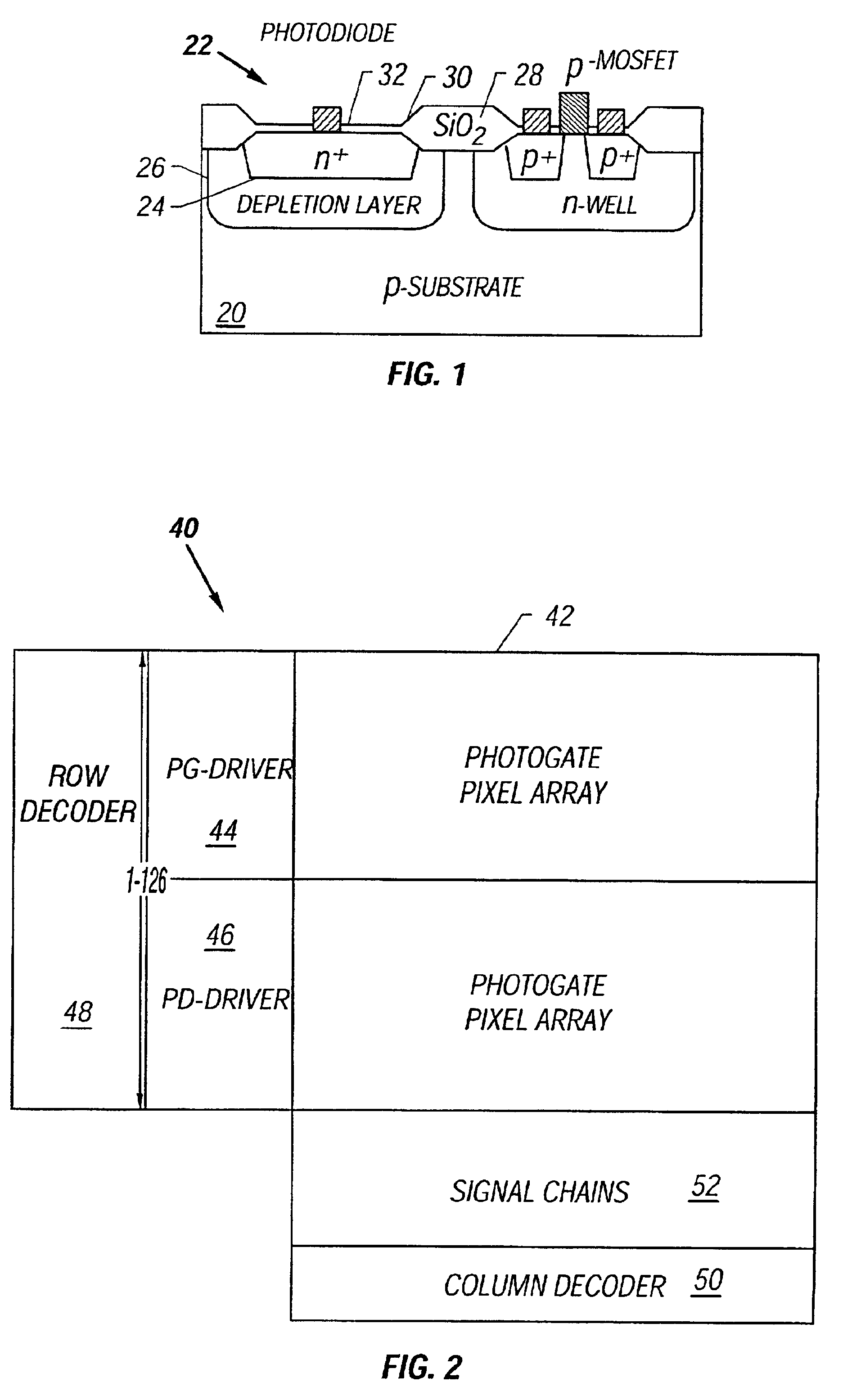
On the other hand, only some of the photoelectrons generated outside the depletion region 26 will diffuse into the collecting area, thereby reducing the collection efficiency and increasing cross-talk.
The increased cross-talk can lead to degraded color performance and smear.
Another problem in imagers made using bulk-CMOS technology is a rise in photodiode leakage current when the device is exposed to radiation.
Although the leakage current can be reduced by using a radiation-hard fabrication process, such processes are relatively expensive and add to the overall cost of the imager.
Nevertheless, the thin silicon film in SOI-MOS devices previously has made them unsuitable for imagers.

Method used


Image

  • Silicon-on-insulator (SOI) active pixel sensors with the photosite implemented in the substrate
  • Silicon-on-insulator (SOI) active pixel sensors with the photosite implemented in the substrate
  • Silicon-on-insulator (SOI) active pixel sensors with the photosite implemented in the substrate

Examples


Embodiment Construction

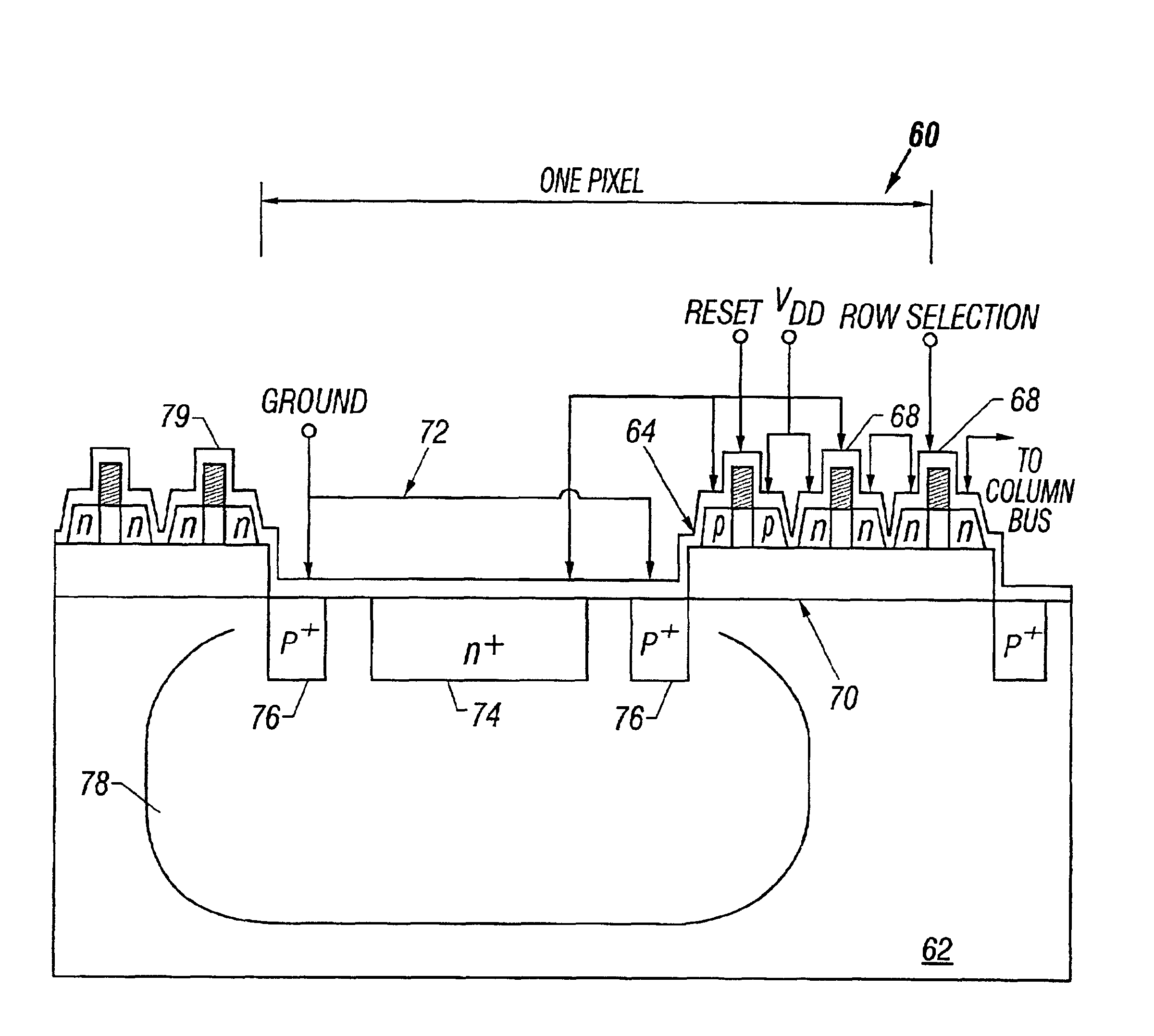
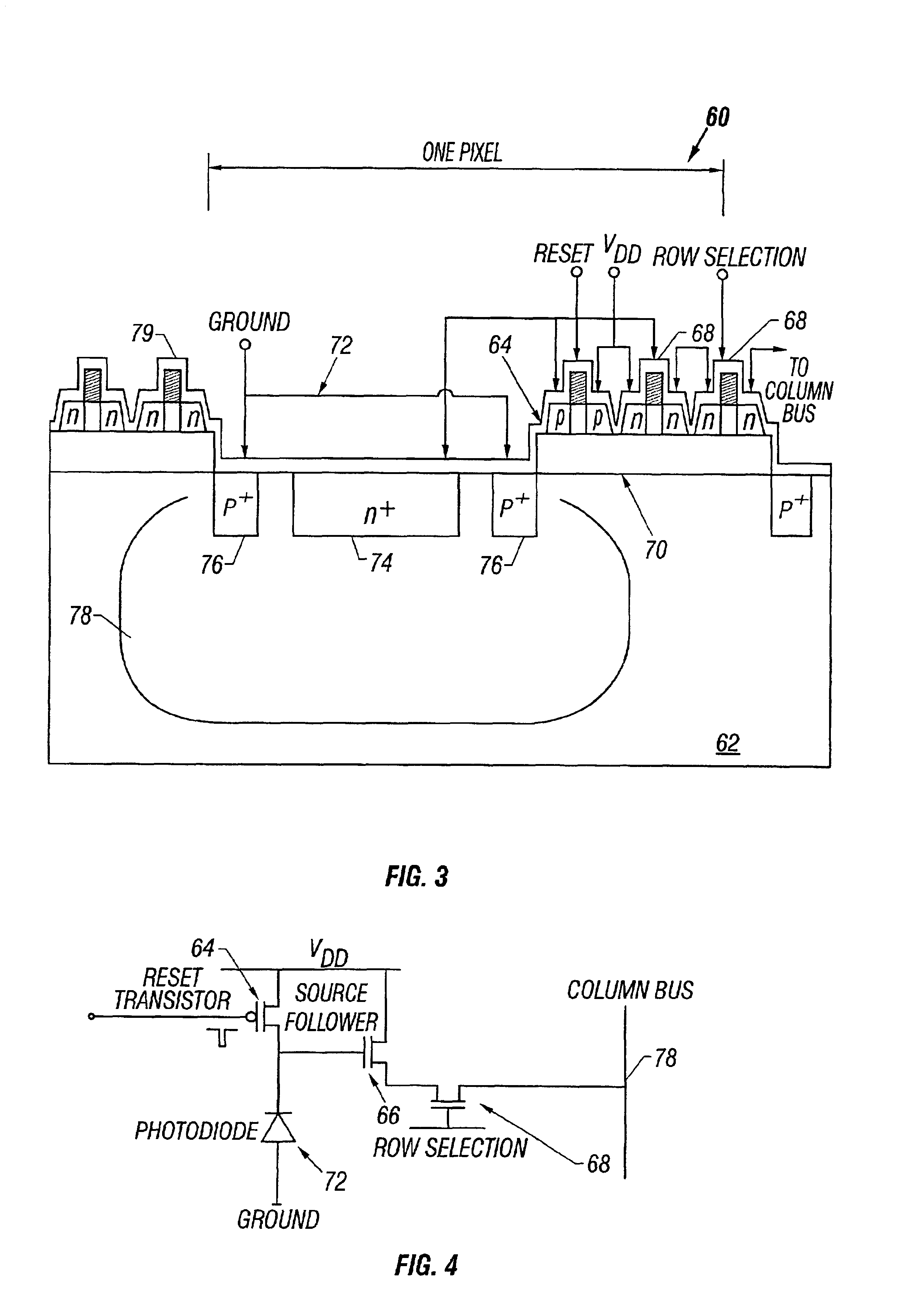
FIG. 2 shows an exemplary active pixel sensor imager 40 formed on an integrated circuit chip that includes an array 42 of active pixel sensors. In one implementation, for example, the imager 40 includes a 144×128 array of pixels. The array 42 can include photogate pixels and / or photodiode pixels. The imager 40 also includes circuitry 44 for driving the photogate pixels and circuitry 46 for driving the photodiode pixels. In addition, the imager 40 has a row decoder 48 for selecting a particular row of pixels and a column decoder 50 for selecting a particular column of pixels, as well as source-follower signal chain circuitry 52. The signal chain circuitry can include, for example, enhancement mode and / or depletion mode source-followers. An on-chip controller (not shown) controls the operation of the decoders 48, 50, the drivers 44, 46 and the pixels.

In general, the imager 40 can be fabricated using a SOI-CMOS process by integrating the photodetectors on the SOI substrate, instead of ...


PUM


Abstract

Active pixel sensors for a high quality imager are fabricated using a silicon-on-insulator (SOI) process by integrating the photodetectors on the SOI substrate and forming pixel readout transistors on the SOI thin-film. The technique can include forming silicon islands on a buried insulator layer disposed on a silicon substrate and selectively etching away the buried insulator layer over a region of the substrate to define a photodetector area. Dopants of a first conductivity type are implanted to form a signal node in the photodetector area and to form simultaneously drain / source regions for a first transistor in at least a first one of the silicon islands. Dopants of a second conductivity type are implanted to form drain / source regions for a second transistor in at least a second one of the silicon islands. Isolation rings around the photodetector also can be formed when dopants of the second conductivity type are implanted. Interconnections among the transistors and the photodetector are provided to allow signals sensed by the photodetector to be read out via the transistors formed on the silicon islands.

Description

BACKGROUNDThe present disclosure relates, in general, to image sensors and, in particular, to silicon-on-insulator (SOI) active pixel sensors with the photosites implemented in the substrate.In general, image sensors find applications in a wide variety of fields, including machine vision, robotics, guidance and navigation, and automotive applications, as well as consumer products. While complementary metal-oxide-semiconductor CMOS) technology has provided the foundation for advances in low-cost, low-power, reliable, highly integrated systems for many consumer applications, charge coupled devices (CCDs) have been, until recently, the primary technology used in electronic imaging applications. CCDs, however, are high capacitance devices that require high voltage clocks, consume large amounts of energy, and provide only serial output. They require specialized silicon processing that is not compatible with CMOS technology.More recently, the availability of near or sub-micron CMOS techno...

Claims


Application Information

Patent Timeline
Patent Type & Authority Patents(United States)
IPC IPC(8): H01L27/146H01L27/12
CPCH01L27/14643H01L27/14609H01L27/12
Inventor ZHENG, XINYUPAIN, BEDABRATA
Owner CALIFORNIA INST OF TECH
Learn More