Semiconductor polysilicon component and method of manufacture thereof

a polysilicon and semiconductor technology, applied in the direction of polycrystalline material growth, crystal growth process, chemically reactive gas growth, etc., can solve the problem of low resistivity comparable to that due insufficient resistivity, and inability to obtain a comparable resistivity to the mbe method, etc. problem, to achieve the effect of improving the reaction with an oxygen gas

Inactive Publication Date: 2005-01-04
TOHOKU TECHNO ARCH CO LTD +1
View PDF2 Cites 220 Cited by
  • Summary
  • Abstract
  • Description
  • Claims
  • Application Information

AI Technical Summary

Benefits of technology

When the hydrative zinc acetyl acetonate is preliminarily heated and decomposed, reactivity with an oxygen gas can be improved. Furthermore, since the zinc acetyl acetonate contains an impurity of I group or III group, an n-type or p-type semiconductor can be obtained.

Problems solved by technology

However, the method is not a preferable method in realizing a low cost and large area active element.
However, low resistivity comparable to that due to the MBE method has not been obtained.
In addition, the resistivity thereof is also insufficient.
Furthermore, there is no report of applications of the fabricating method to other elements.
However, the crystallinity is not sufficient.
As a result, there occurs a structural problem that the transparent transistor does not at all work.
However, it does not mean that the above structural problem caused in applying to the transparent transistor can be improved.

Method used


Image

  • Semiconductor polysilicon component and method of manufacture thereof
  • Semiconductor polysilicon component and method of manufacture thereof
  • Semiconductor polysilicon component and method of manufacture thereof

Examples


embodiment 1

(Embodiment 1)

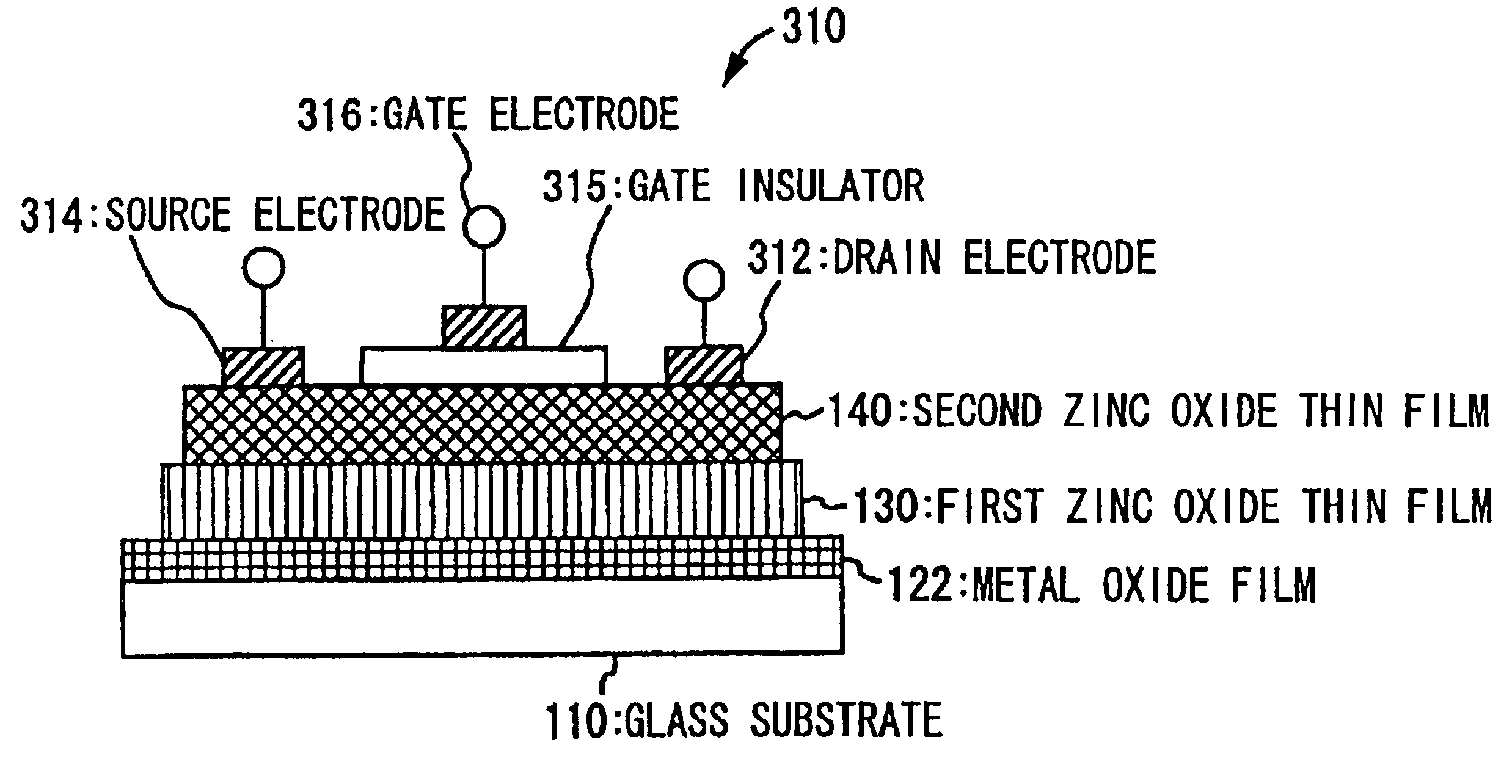
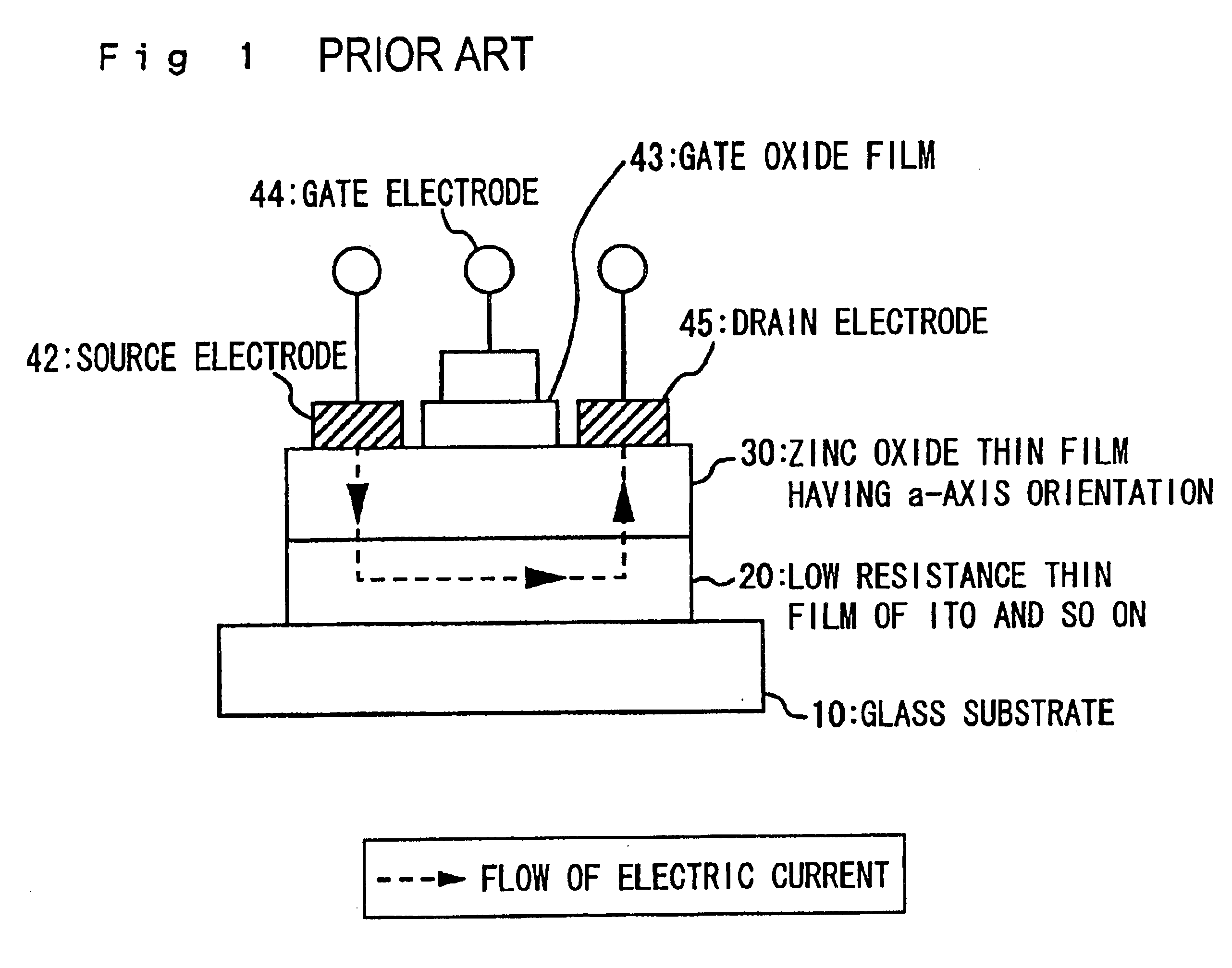
In FIGS. 14A and 14B, an example in which the member is applied to a transparent transistor is shown. FIG. 14A is a sectional view of a transistor 310. The orientation of a used zinc oxide thin film is an a-axis that is an orientation axis best fitted to a flow of a current of the transparent transistor. A thickness of a first zinc oxide thin film 130 formed on a glass substrate 110 is in the range of 500 to 1,500 angstrom, and is preferable to be 1,000 angstrom. An n conductivity type is shown by diffusion of Al atoms from an Al thin film that is deposited at an interface and used to apply a DC bias. A film thickness of an oxide of Al after the oxidation of the metal Al is in the range of 200 to 400 angstrom. A film thickness of a second zinc oxide thin film 140 is in the range of 1,000 to 2,000 angstrom, and is preferable to be 1,500 angstrom. Li is added to the second zinc oxide thin film, and thereby zinc oxide showing a value of the resistivity of 106 Ω·cm is depo...

embodiment 2

(Embodiment 2)

The transparent transistor 310 shown in Embodiment 1 has the gate electrode in an upper portion thereof, in contrast, in a transistor 320 shown in Embodiment 2 of FIG. 14B, a gate electrode 326 is formed in a lower portion. The transistor 320 has features in that the transistor is less affected by an external circumstance and, since a member of the transistor is formed after a high quality gate insulating film is formed, the transistor is less influenced by the hysteresis due to a gate voltage fluctuation. All of the features and film thicknesses of the respective thin films become the same as that of Embodiment 1. The transparent transistor of this configuration allows further reducing an off-voltage than that of Embodiment 1.

embodiment 3

(Embodiment 3)

Embodiment 3 relates to a transparent transistor less affected by high temperatures and radiation. In a transistor made of Si or Ge, there is a problem in that, being narrow in a width of the forbidden band, owing to high temperatures or radiation, electrons in a filled band are excited to a conduction band, resulting in incapability of controlling by the gate voltage. The zinc oxide thin film has a width of the forbidden band of 3.2 eV that is twice as that of Si. Accordingly, the transistor that uses the zinc oxide thin film can be less affected by the high temperatures or radiation. However, when an oxide film of a material into which Al or Sn can easily diffuse is used, a metal component diffuses into zinc oxide, resulting in easily causing defects due to change of properties with time. Accordingly, as a structure of the transparent transistor that uses the zinc oxide thin film, though similar to that shown in FIGS. 14A and 14B, with an oxide film of tungsten (W) o...


PUM

PropertyMeasurementUnit
transmittanceaaaaaaaaaa
thicknessaaaaaaaaaa
transmittanceaaaaaaaaaa

Abstract

On a transparent substrate, by use of, for instance, vapor deposition, an Al film is formed. Subsequently, with a DC-bias applied on a surface of the Al film, a first zinc oxide thin film is formed by use of a sputtering method. On a surface of the first zinc oxide thin film, according to an atmospheric MO-CVD method, a second zinc oxide thin film is formed. When the second zinc oxide thin film deposited by use of an MO-CVD method is formed on the first zinc oxide thin film having a-axis orientation, the second zinc oxide thin film becomes to have the a-axis orientation. Since the Al thin film, owing to heat during the deposition by use of the MO-CVD method, is absorbed in the first zinc oxide thin film, the transparency is improved. As a result, a sample having a ZnO/ZnO/Al/glass structure becomes high in the transparency as a whole.

Description

TECHNICAL FIELDThe present invention relates to a semiconductor member suitable for constituting a transparent semiconductor element, in particular, to zinc oxide that is high in the transparency and low in the resistivity.BACKGROUND ARTA polycrystalline zinc oxide member whose constituent elements are zinc and oxygen is expected to apply in a photo-detector, a surface acoustic wave element, a piezoelectric element, a transparent conductive electrode and an active element. As a method of fabricating the same, many methods such as an MBE method in an ultra-high vacuum, a laser aberration method, a sputtering method, a vacuum deposition method, a sol-gel method, and an MO-CVD method are under study.As to an active element such as a transparent transistor and so on, from a point of view of the crystallinity, a method in which the MBE method in an ultra-high vacuum and the laser aberration method are combined is a present main stream. However, the method is not a preferable method in re...

Claims


Application Information

Patent Timeline
Patent Type & Authority Patents(United States)
IPC IPC(8): C03C17/36C23C14/08C23C14/02C30B25/02C23C16/40H01L29/786
CPCC03C17/3417C03C17/36C03C17/3605C03C17/3615C03C17/3649C03C17/3671C23C14/025H01L29/7869C23C14/086C23C16/40C23C16/407C30B25/02C30B29/16H01L29/786
Inventor HAGA, KOICHI
Owner TOHOKU TECHNO ARCH CO LTD
Why Eureka
Try Eureka