Semiconductor device having source/channel or drain/channel boundary regions

a semiconductor device and drain technology, applied in the direction of semiconductor devices, electrical devices, transistors, etc., can solve the problems of poor drain voltage resistance, reverse current leakage from the drain to the source, and the insulated gate fet of the type above often suffers problems, so as to improve the voltage resistance

Inactive Publication Date: 2005-01-04
SEMICON ENERGY LAB CO LTD
View PDF57 Cites 23 Cited by
  • Summary
  • Abstract
  • Description
  • Claims
  • Application Information

AI Technical Summary

Benefits of technology

[0012]An object of the present invention is to provide a semiconductor device comprising an insulated gate FET free from problems such as the leakage of reverse current from the drain to the source, and the low drain voltage resistance, which both had been the problems of the prior art insulated gate FETs.
[0023]The insulated gate FET according to the present invention is characterized by that a region having added carbon, nitrogen, or oxygen to realize a wide band gap is established at the area to which an electric field concentrates, e.g., at the vicinity of the boundary between the channel and the drain, to obtain a high band gap which is capable of avoiding leakage of the carriers. It can be thus seen clearly that the present invention is based on a concept completely different from the conventional concept based on the relaxation of the electric field concentration.
[0025]Further, the present invention has a feature that the location of the wide band gap can be shifted by changing the location of the region adding thereto the impurity such as carbon, nitrogen, and oxygen. Of course, the resistance becomes large in the region to establish a wide band gap, resulting in the relaxation of electric field concentration.
[0026]It is needless to say that combining the present invention with the known LDD structure, and further combining the above structure with the SDD (side doped drain) structure in which a channel forming region is formed in trapezoid shape protrusion of a substrate makes it possible to further improve the device characteristic.
[0027]In the structure shown in FIG. 17, the impurity for activating the semiconductor is doped, extending to the boundaries 312 and 313. However, when the impurity is doped within the source region and drain region 305 and 306 only and a very small amount of oxygen (at 1018 to 1021 atoms per 1 cm3) is doped to the ODD regions 309 and 310, these oxygen atoms become donors in the semiconductor such as silicon and impart the weak N type conductivity to the semiconductor, so that in the case of NMOS in which the source and drain regions have the N type conductivity it is possible to make it seemingly have a LDD structure. Further, since oxygen atoms themselves hardly diffuse in a semiconductor compared with the usual impurity element such as phosphorus, boron, and arsenide, the problem caused in the conventional LDD structure can be prevented, i.e. the problem that the channel region is contaminated due to the diffusion of the impurity element from the source and drain regions including LDD regions and a current flow is continuously formed between the source and the drain in the channel. This process makes it possible to elevate the productivity of the insulated gate FET having a channel length not longer than sub-microns, specifically not longer than quarter-microns. In the above case of doping a very small amount of oxygen too, the punch through current can be prevented by providing the ODD regions 309 and 310 in the portions deeper than the locations of the source region 305 and the drain region 306.
[0029]Naturally, the structure according to the present invention can be applied to any type of the insulated gate FETs such as those of a stagger type, an inverted stagger type, a planar type, and an inverted planar type, to improve voltage resistance between the source and the drain and to avoid the occurrence of a punch-through current. The device according to the present invention not only is applicable to an insulated gate FET, but also is applicable to various other semiconductor devices and is effective to overcome problems (such as the problem of throw leakage) which originate from a local concentration of the electric field.

Problems solved by technology

However, in those types of insulated gate FETs, there have occurred problems such as the reverse current leakage from the drain to the source, and the poor drain voltage resistance.
More specifically, as is illustrated in FIG. 2, an insulated gate FET of the type above often suffers problems ascribed to the reverse current leakage.
If an insulated gate FET having a VD-ID curve (B) in FIG. 3 were to be fabricated, a drain current will flow continuously to result in a throw leakage state even though a voltage well below the threshold voltage were to be applied to the gate electrode.
This would result in a switching device having poor reliability and insufficient performance.
In this process, however, the impurity having doped for imparting one conductivity type to a part of the semiconductor layer diffuses from the drain and the source that there still remains a problem to be solved.
For an insulated gate field effect transistor in which the channel length is not longer than sub-microns, this becomes a major problem.
That is, there is a problem that a current flow is continuously formed between the source and the drain in the channel forming region due to diffusion of impurities from the source and the drain to the channel forming region.

Method used


Image

  • Semiconductor device having source/channel or drain/channel boundary regions
  • Semiconductor device having source/channel or drain/channel boundary regions
  • Semiconductor device having source/channel or drain/channel boundary regions

Examples


example 1

[0058]This example provides a method for fabricating a semiconductor device on a substrate. According to the method, the patterning to form a gate electrode on a gate insulating film and the formation of an opening for adding therethrough at least one element selected from the group consisting of carbon, nitrogen, and oxygen are carried out at the same time. Then, the above element is added through the opening and the gate electrode is completed. By the above procedure, the region having added thereto at least one element selected from the group consisting of carbon, nitrogen, and oxygen is provided in the periphery of the semiconductor layer below the gate electrode, or between the semiconductor layer below the gate electrode and the source and drain.

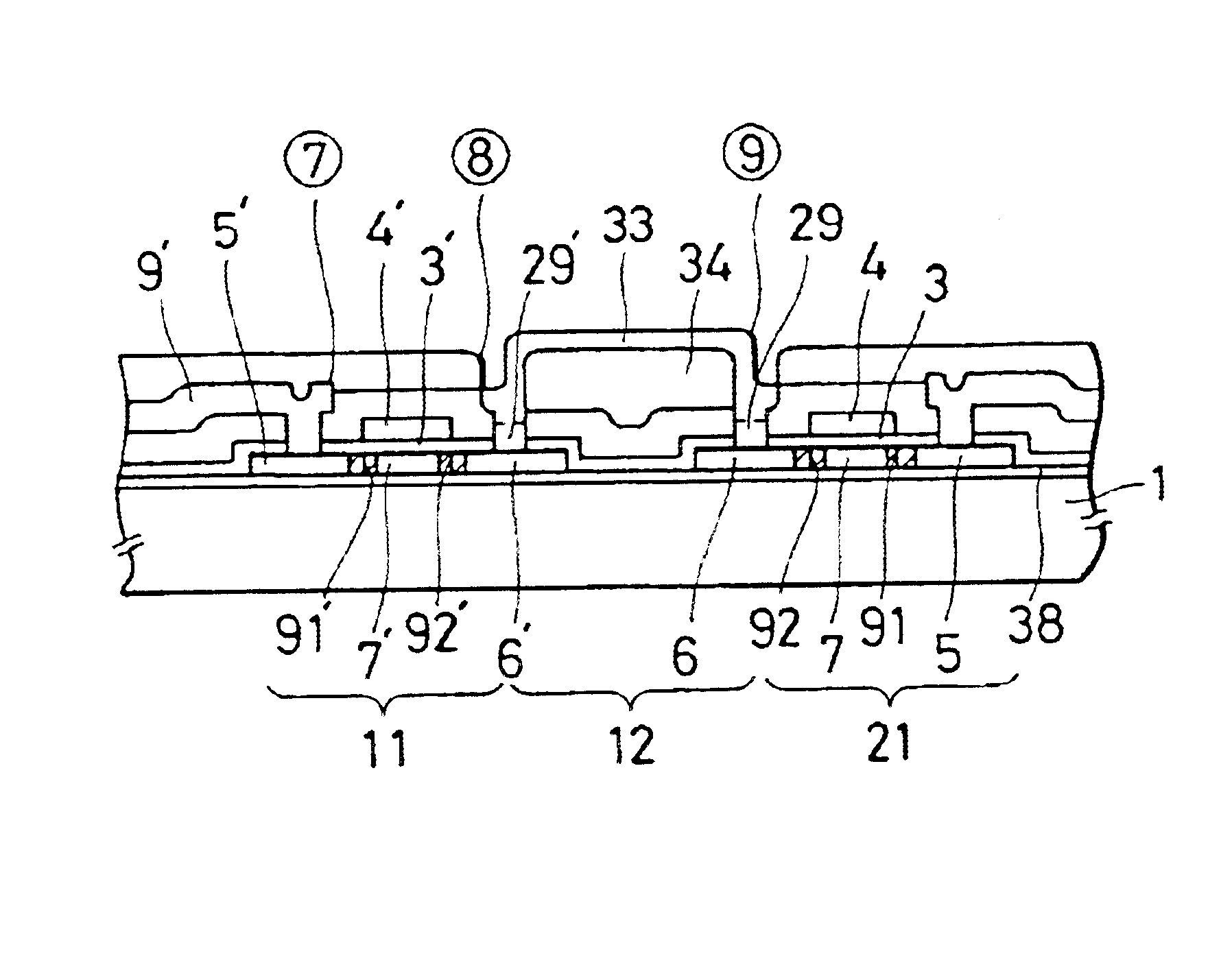
[0059]Referring to FIG. 6, a process for fabricating a complementary TFT (C / TFT) pair is described. The C / TFT pair comprises an n-channel TFT and a p-channel TFT provided on a glass substrate at a complementary structure. The symbols o...

example 2

[0097]This example provides another method for fabricating a semiconductor device on a substrate. The method comprises the step of patterning a resist, semiconductor, insulator, or metal, or a complex thereof together with forming an opening for adding at least one element selected from the group consisting of carbon, nitrogen, and oxygen; and the step of adding at least one element selected from the group consisting of carbon, nitrogen, and oxygen. For example, it is used as a method for fabricating a C / TFT pair shown in FIG. 9(C). The difference between the process in EXAMPLE 1 and the present process is that the process of EXAMPLE 1 comprises a step of ion-doping the impurities such as carbon, nitrogen, and oxygen to the semiconductor layer 2 and 2′ using gate electrodes 4 and 4′ as well as the resist films thereon as the masks (see FIGS. 6 (B) and 6 (C)), whereas the process of the present EXAMPLE comprises ion-doping first the impurities such as carbon, nitrogen, and oxygen to ...

example 3

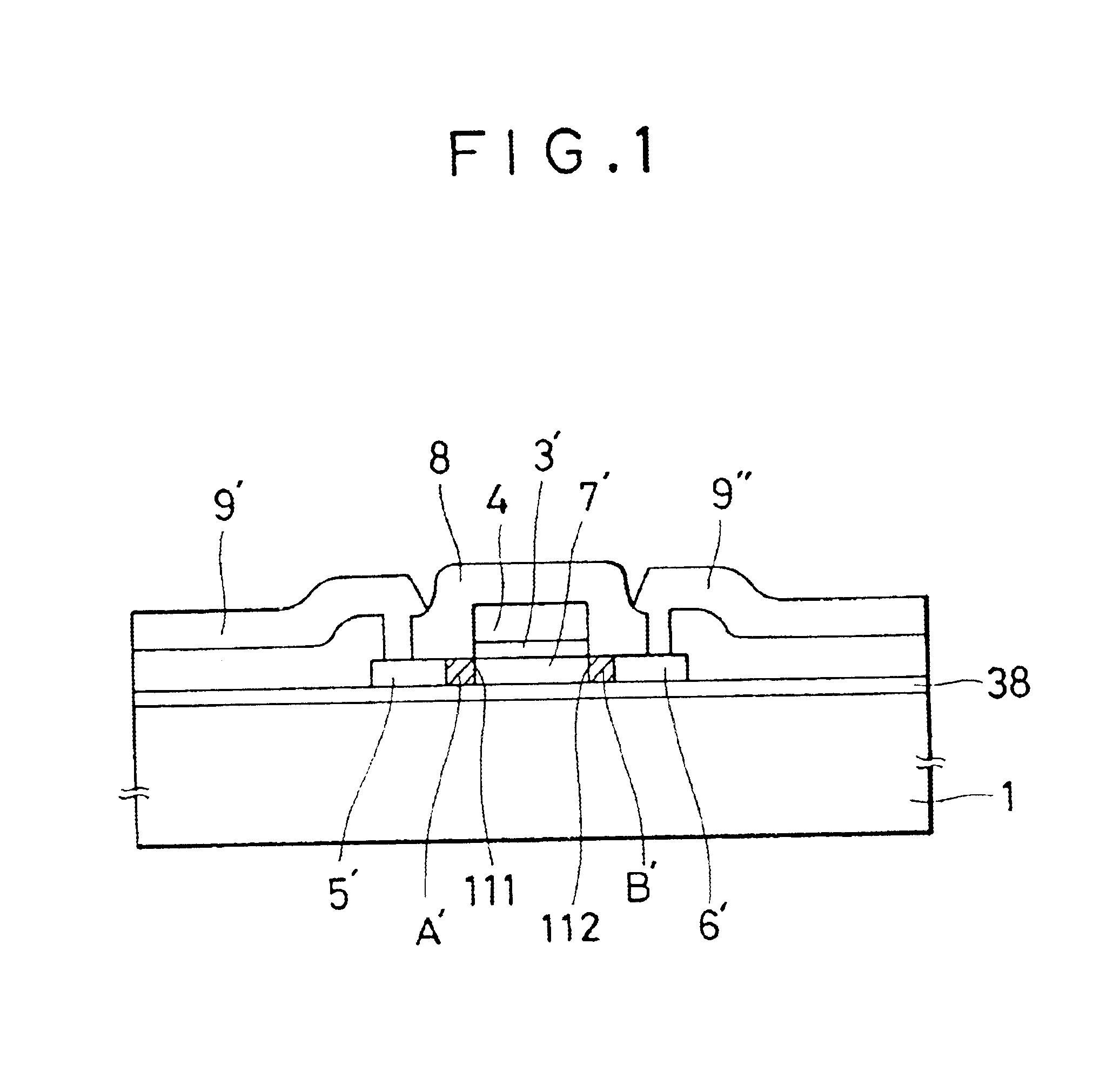
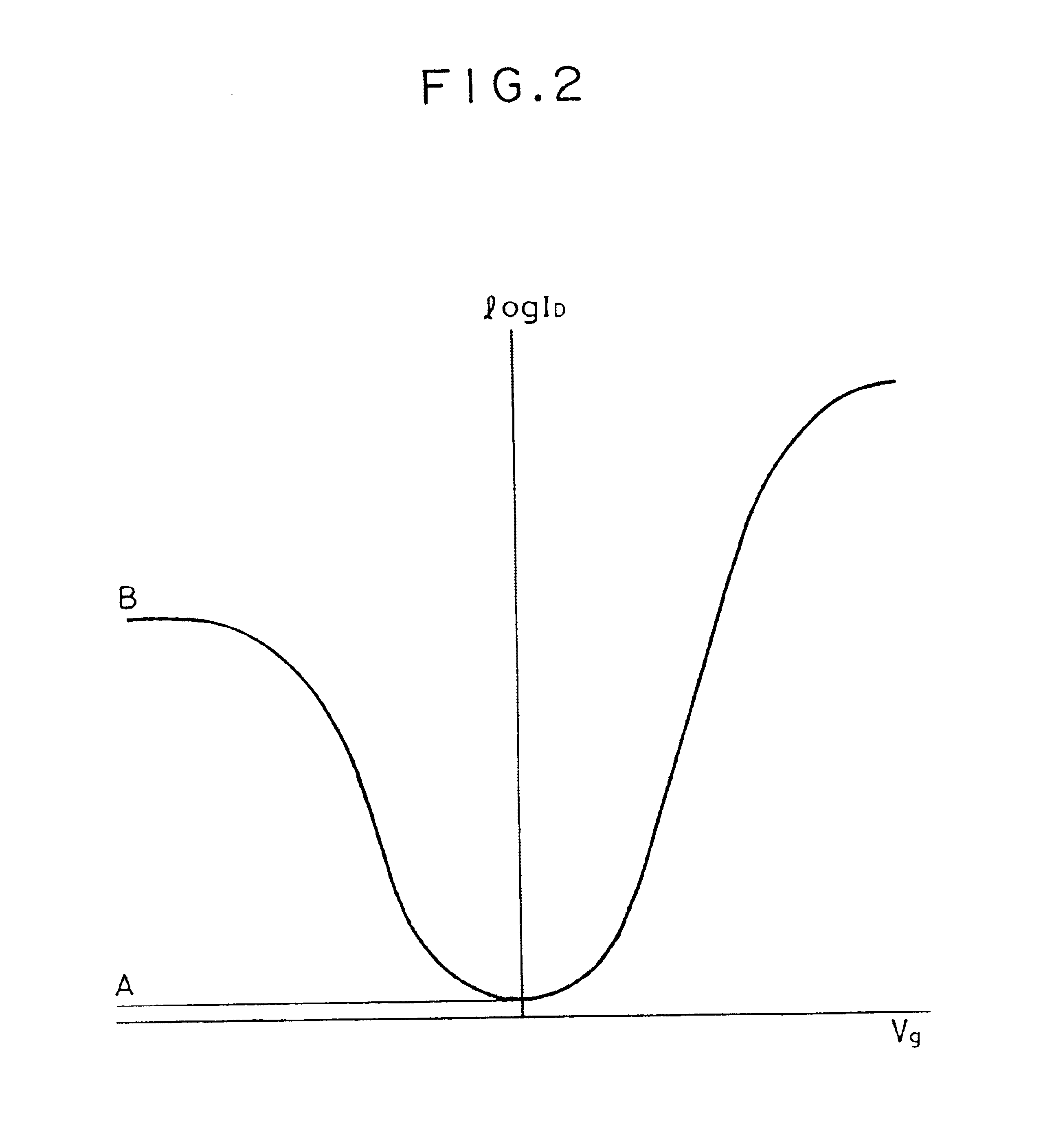
[0106]Referring to FIG. 25, a TFT similar to that fabricated in EXAMPLE 2 is described, only that the TFT of the present EXAMPLE comprises the impurity regions at the vicinity of the surface of the semiconductor layer. The structure thus obtained also is increased in the voltage resistance between the source and the drain. Those impurities, of course, may be present deep inside the semiconductor layer to the vicinity of the substrate, but the structure of the present EXAMPLE is advantageous in that the impurities such as carbon, nitrogen, and oxygen can be doped with a lower ion energy as compared with the processes of EXAMPLES 1 and 2. Furthermore, ion intrusion to undesired areas can be avoided. In the FIGURE, the numerals and the symbols are the same as those used in FIG. 1. Both a p-channel type and a n-channel type naturally can be used as the insulated gate FET described herein.

[0107]An insulated gate FET was thus fabricated by following the same process as described in EXAMPL...


PUM


Abstract

A semiconductor device and a method for forming the same are disclosed. The semiconductor device comprising an insulated gate field effect transistor provided with a region having added thereto an element at least one selected from the group consisting of carbon, nitrogen, and oxygen, said region having established at either or both of the vicinity of the boundary between the drain and the semiconductor layer under the gate electrode and the vicinity of the boundary between the source and the semiconductor layer under the gate electrode for example by ion implantation using a mask. It is free from the problems of reverse leakage between the source and the drain, and of throw leakage which occurs even at a voltage below the threshold ascribed to the low voltage resistance between the source and the drain.

Description

[0002]This is a Divisional application of Ser. No. 08 / 213,837, filed Mar. 16, 1994 now U.S. Pat. No. 5,821,563; which itself is a continuation of Ser. No. 07 / 813,071, filed Dec. 26, 1991 now abandoned.BACKGROUND OF THE INVENTION[0003]1. Field of the Invention[0004]The present invention relates to an insulated gate field effect semiconductor device (FET) for use in switching devices, integrated circuits (ICs), and display devices such as liquid crystal displays and the like.[0005]2. Description of the Prior Art[0006]Insulated gate FETs heretofore fabricated unexceptionally comprise a semiconductor region in which a source, a channel, and a drain are established. In such insulated gate FETS, the drain is in contact with the channel and the source is in contact with the channel. However, in those types of insulated gate FETs, there have occurred problems such as the reverse current leakage from the drain to the source, and the poor drain voltage resistance.[0007]More specifically, as i...

Claims


Application Information

Patent Timeline
Patent Type & Authority Patents(United States)
IPC IPC(8): H01L21/265H01L21/336H01L21/77H01L21/8238H01L21/84H01L27/12H01L29/08H01L29/167H01L29/78H01L29/786
CPCH01L21/26506H01L21/823814H01L27/1214H01L27/1222H01L29/0847H01L29/167H01L29/6659H01L29/66757H01L29/7833H01L29/78618H01L29/78675H01L2029/7863
Inventor YAMAZAKI, SHUNPEITAKEMURA, YASUHIKO
Owner SEMICON ENERGY LAB CO LTD
Why Eureka
Try Eureka