Single-chip data processing apparatus incorporating an electrically rewritable nonvolatile memory and method of operating the same

a data processing apparatus and single-chip technology, applied in the field of integrated circuit data processing apparatus, can solve the problems of limiting the chip size reduction advantage of the microcontroller, inactivity of the rom, and inability to reprogramme the program stored in the mask rom, so as to achieve the effect of small chip size and lower cos

Inactive Publication Date: 2005-01-04
SAMSUNG ELECTRONICS CO LTD
View PDF11 Cites 98 Cited by
  • Summary
  • Abstract
  • Description
  • Claims
  • Application Information

AI Technical Summary

Benefits of technology

A general object of the present invention is to provide an on-board pro...

Problems solved by technology

Thus, a program stored in mask ROM cannot be reprogrammed.
However, the ROM of the prior art microcontroller is active only for an on-board writing mode; that is, the ROM is inactive for the other operation modes.
Acc...

Method used


Image

  • Single-chip data processing apparatus incorporating an electrically rewritable nonvolatile memory and method of operating the same
  • Single-chip data processing apparatus incorporating an electrically rewritable nonvolatile memory and method of operating the same
  • Single-chip data processing apparatus incorporating an electrically rewritable nonvolatile memory and method of operating the same

Examples


first embodiment

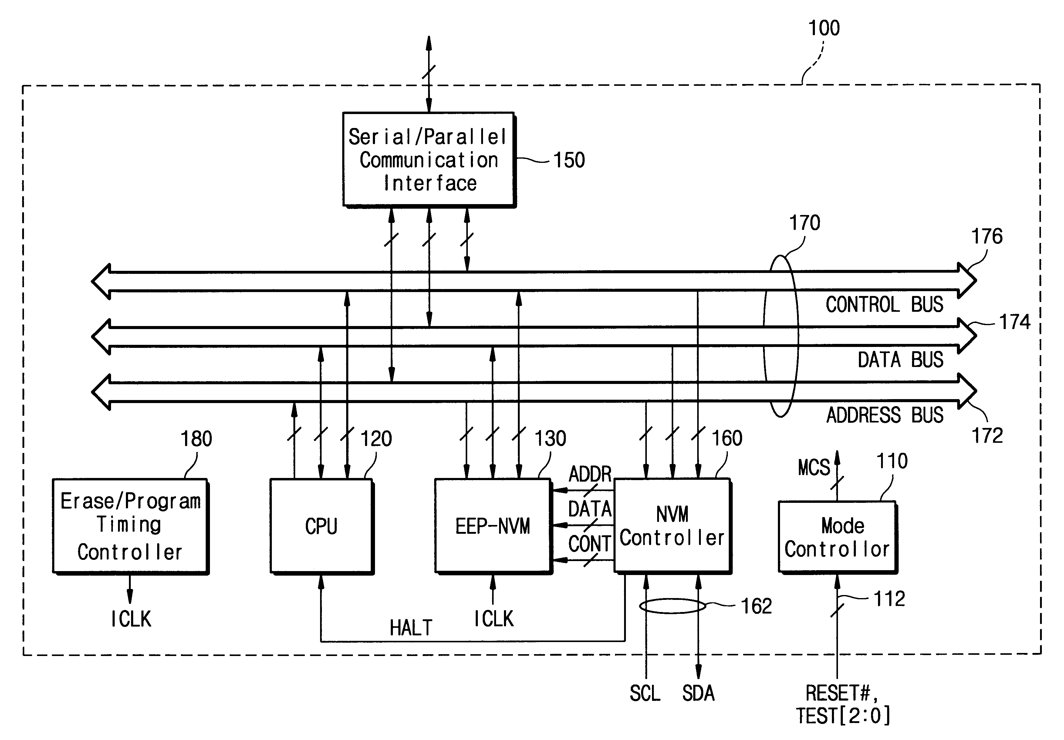
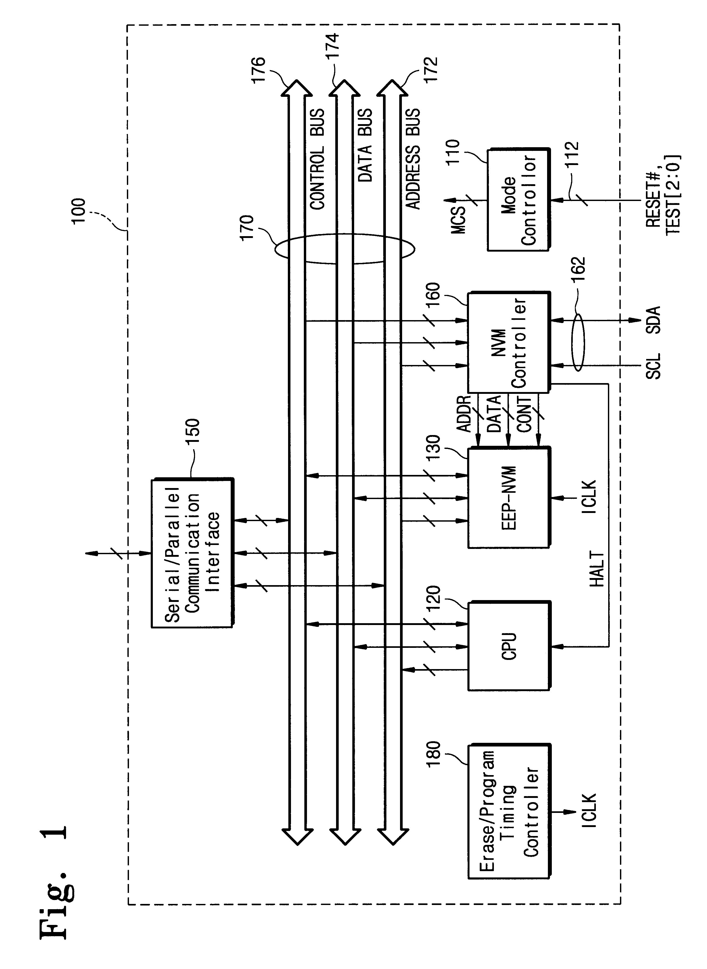
FIG. 1 illustrates a microcontroller 100 according to the present invention. With reference to FIG. 1, the microcontroller 100 is a single chip data processing apparatus of, e.g., 32 bits. The microcontroller 100 comprises a mode controller 110, a central processing unit (CPU) 120, and an electrically erasable and programmable nonvolatile semiconductor memory (EEP-NVM) 130, such as a EEPROM or a flash EEPROM, used as a program memory of the microcontroller 100. The CPU 120 and the EEP-NVM 130 are connected to buses 170 including an address bus 172, a data bus 174 (e.g., of 32 bits), and a control bus 176.

The mode controller 110 receives mode select signals RESET#, TEST0, TEST1 and TEST2 applied from outside of the microcontroller 100 via an input port 112, and generates mode control signals MCS for setting various operation modes in each section of the microcontroller 100. Preferably, MCS is derived from a logical combination of the mode select signals RESET# and TEST0-TEST2. The op...

second embodiment

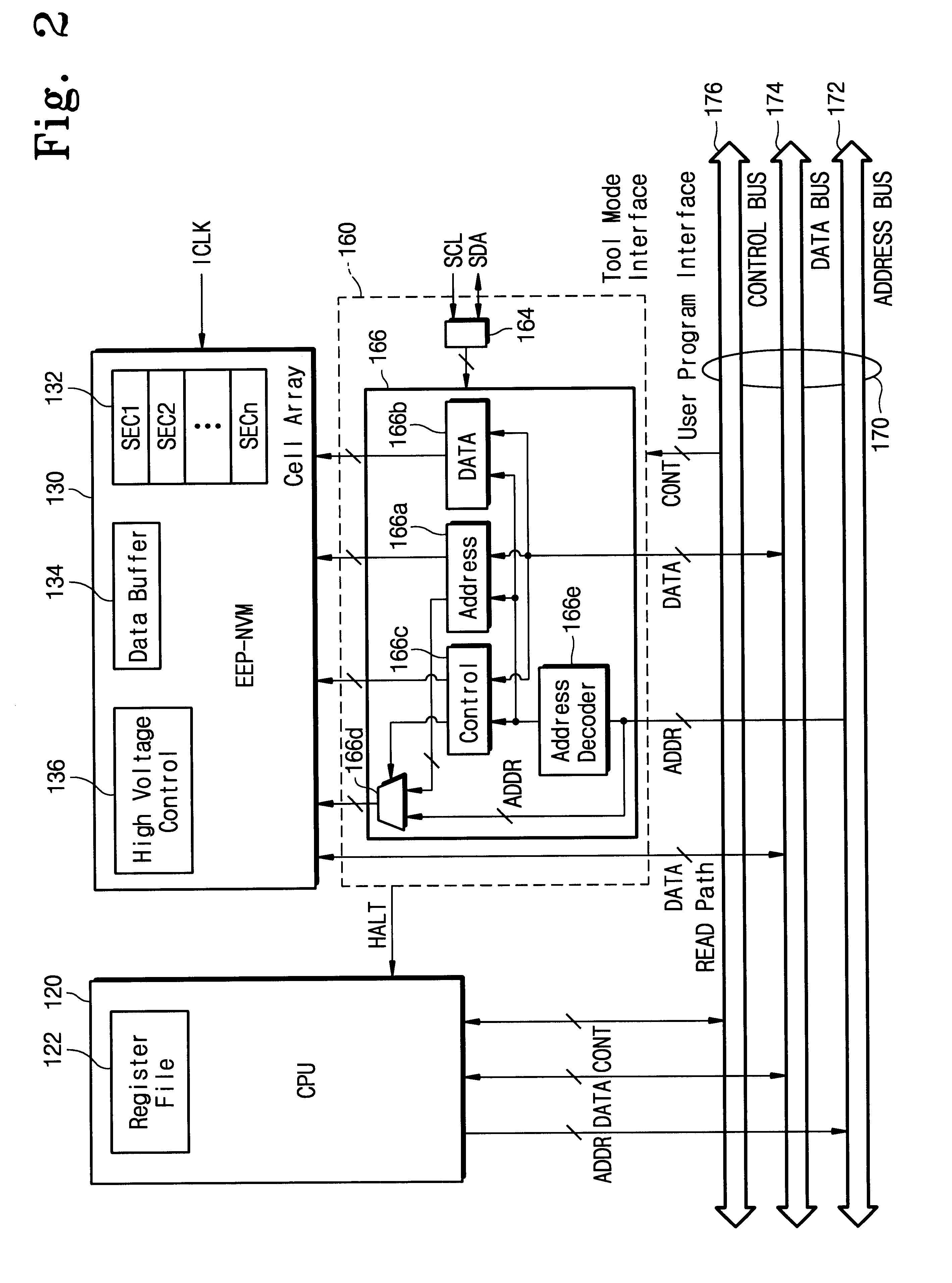
FIG. 8 illustrates another microcontroller 100′ according to the present invention. As can be seen in FIG. 8, the microcontroller 100′ has substantially the same arrangement as that shown in FIG. 1, except that the microcontroller 100′ further includes a buffer RAM 190, such as a static RAM (SRAM) or a ferroelectric RAM (FRAM), and I / O ports 140 is shown for usage in lieu of or in addition to communication interface 150. The buffer memory 190 is connected to the buses 170 and can be used to temporarily store data, such as an update program, such as during the user programming mode in which the update program (i.e., a partial control program) is written into the EEP-NVM 130. In this case, the CPU 120 sets the control register circuit 166c of the NVM controller 160 (see FIG. 2), so that the data stored in the buffer memory 190 is written into the EEP-NVM 130 via the NVM controller 160. In addition, the buffer memory 190 is deactivated by the mode controller 110, together with CPU 120,...


PUM


Abstract

A microcontroller includes an electrically erasable and programmable nonvolatile memory and a memory controller for controlling the nonvolatile memory. Upon writing a control program for the microcontroller and data into the nonvolatile memory pursuant to an externally provided NVM command or an internally issued program command, a CPU of the microcontroller does not intervene in controlling the nonvolatile memory. Particularly, in a programming mode set by the external program command, CPU, buses, and communication interfaces of the microcontroller are deactivated. Further, the memory controller receives a NVM command, an address and data from outside of the microcontroller for controlling an operation of the nonvolatile memory based on the NVM command and the address without intervention of the CPU.

Description

CROSS-REFERENCE TO RELATED APPLICATIONSThis application claims foreign priority to Korean Patent Application Numbers 1999-45785, filed on Oct. 21, 1999; and 2000-61457, filed on Oct. 19, 2000.BACKGROUND OF THE INVENTION1. Field of the InventionThe present invention relates to an integrated circuit data processing apparatus and, more particularly, to a data processing apparatus having an embedded electrically rewritable nonvolatile semiconductor memory.The present invention further relates to methods of operating an integrated circuit data processing apparatus having an embedded electrically rewritable nonvolatile semiconductor memory.2. Description of the Related ArtThe use of VLSI chip circuitry in digital data processing systems, or computers, has realized the benefits of smaller size, lighter weight, lower cost, reduced power requirements, and higher reliability. VLSI circuitry such as single-chip computers (i.e., microcontrollers or microcontrollers) allow computer electronics t...

Claims


Application Information

Patent Timeline
IPC IPC(8): G05B19/04G05B19/042G06F9/445G11C16/02
CPCG05B19/0426G06F8/60G05B2219/23308G05B2219/23345Y02B60/183G05B2219/25341G05B2219/25265Y02D10/00G11C16/02
Inventor AHN, JONG-KEUNYU, BUM-SEOKRA, SANG-JOOKIM, JONG-IN
Owner SAMSUNG ELECTRONICS CO LTD
Why Eureka
Try Eureka