
Non-volatile memory cell fabricated with slight modification to a conventional logic process and methods of operating same

a non-volatile memory and logic process technology, applied in the field of non-volatile memory, can solve the problems of complex process, incompatibility with conventional logic process, and high cost, and achieve the effect of improving operating margin, suppressing leakage current, and improving electron removal operation and normal read operation

Inactive Publication Date: 2005-01-11
MOSYS INC
View PDF34 Cites 27 Cited by
  • Summary
  • Abstract
  • Description
  • Claims
  • Application Information

AI Technical Summary

Benefits of technology

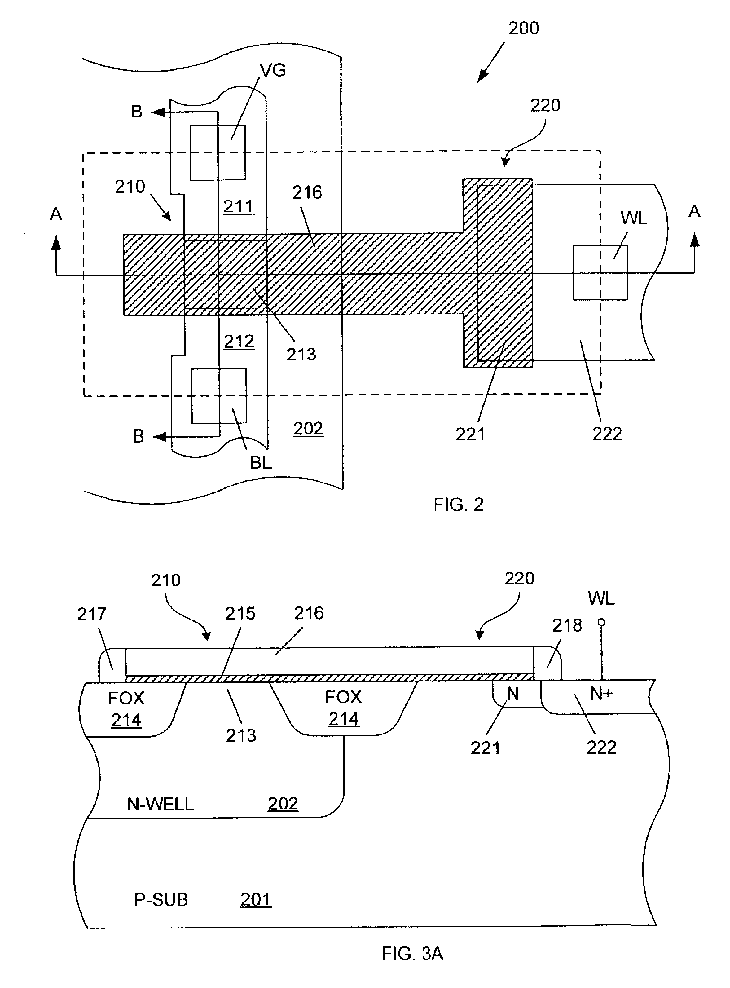
In one embodiment, the non-volatile memory cell includes a p-type semiconductor substrate and an n-well located in the substrate. A PMOS transistor is fabricated in the n-well. The PMOS transistor includes the thin gate oxide and an overlying polycrystalline silicon gate. An NMOS capacitor structure is fabricated in the p-type substrate. The NMOS capacitor structure includes an n-type coupling region located in the p-type substrate. The n-type coupling region is formed by the n-type source / drain implants, thereby eliminating the need for any additional implants not normally provided by the conventional logic process. The thin gate oxide and the polycrystalline silicon gate extend over the p-type substrate and the n-type coupling region, thereby forming the NMOS capacitor structure. The NMOS capacitor structure and the PMOS transistor are sized such that the NMOS capacitor structure has a capacitance larger than a capacitance of the PMOS transistor. Advantageously, a triple-well structure is not required by the present invention.
The present invention incorporates a negative voltage generator that provides a negative boosted voltage having a voltage level that is less than the Vss supply voltage by a voltage that is less than a diode turn-on voltage (0.7 Volts). In one embodiment, the negative boosted voltage has a value of −0.5 Volts. The negative boosted voltage is applied to the control gate of the non-volatile memory cell to enhance the electron removal operation and normal read operation without requiring a triple-well underneath the control gate.
The present invention also incorporates a positive voltage generator that provides a positive boosted voltage having a voltage level that is greater than the Vdd supply voltage by a voltage that is less than a diode turn-on voltage (0.7 Volts). In one embodiment, the positive boosted voltage has a value equal to Vdd+0.5 Volts. The positive boosted voltage is applied to the N-well of the non-volatile memory cell and the control gates of non-selected memory cells during normal read operations to suppress leakage currents through those non-selected memory cells and to improve operating margins.
In accordance with one embodiment of the present invention, non-volatile memory cells are used in a system-on-a-chip system. After power-up of a system-on-a-chip integrated circuit incorporating the embedded non-volatile memory cells, the contents of the non-volatile memory cells are read out and stored (with or without data decompression operations) into on-chip or off-chip volatile memory. The data contents of the non-volatile memory cells are then refreshed (through charge injection and removal) with optimum signal condition. The non-volatile memory cells then remain in an idle or standby mode substantially without a significant external electric field. If a reprogramming operation or a refresh operation is required, then the non-volatile memory cells are reprogrammed or refreshed as required and then returned to the idle or standby mode. As a result, the storage characteristics of the thin oxide non-volatile memory cells are improved.

Problems solved by technology

However, traditional nonvolatile memory processes, which typically use stacked gate or split-gate memory cells, are not compatible with a conventional logic process.
The combination of a nonvolatile memory process and a conventional logic process results in much more complicated and expensive “merged non-volatile memory and logic” process to implement system-on-chip integrated circuits.
This is undesirable because the typical usage of the non-volatile memory block in an SOC application is small in relation to the overall chip size.
This process is therefore more complex than a conventional logic process, which requires only a single layer of polysilicon.
The use of an n-well as the control gate and the need for an injector region result in a relatively large cell size.
erations. This additional implant is not available in a standard logi
control gate). Both the extra n+ implant and the triple-well are not available in a conventional
Such a thick tunneling oxide is not compatible with conventional logic processes, because conventional logic processes provide for logic transistors having a gate oxide thickness of about 5 nm for a 0.25 micron process and 3.5 nm for a 0.18 micron process.
These high voltage transistors are not available in a conventional logic process.
However, this memory cell only supports programming (i.e., electron injection into the floating gate).
The use of a thin gate oxide as tunneling oxide presents a challenge for achieving acceptable data retention time for non-volatile memory cells.
Although programming voltages may be reduced by the use of a thin gate oxide, the thin gate oxide will exacerbate cell disturbances.
That is, the thin gate oxide will significantly increase the probability of spurious charge injection or removal from the floating gate during normal program, erase and read operations.
As a result, data-retention becomes a serious problem when using the standard gate oxide as the tunnel oxide in a non-volatile memory cell.

Method used


Image

  • Non-volatile memory cell fabricated with slight modification to a conventional logic process and methods of operating same
  • Non-volatile memory cell fabricated with slight modification to a conventional logic process and methods of operating same
  • Non-volatile memory cell fabricated with slight modification to a conventional logic process and methods of operating same

Examples


Embodiment Construction

FIG. 2 is a top layout view of a non-volatile memory cell 200 in accordance with one embodiment of the present invention. FIG. 3A is a cross sectional view of the non-volatile memory cell of FIG. 2 along section line A—A. FIG. 3B is a cross sectional view of the non-volatile memory cell of FIG. 2 along section line B—B. In the described example, non-volatile memory cell 200 is fabricated using a 0.25 micron conventional logic process having a typical gate oxide thickness of about 5 nm. Non-volatile memory cell 200 is operated in response to a positive Vdd supply voltage that has a nominal voltage of 2.5 Volts during normal operations, and a Vss supply voltage of 0 Volts.

Non-volatile memory cell 200 is fabricated in a p-type monocrystalline semiconductor substrate 201 (see FIGS. 3A and 3B). In the described embodiment, substrate 201 is silicon. Non-volatile memory cell 200 includes a PMOS access transistor 210. Access transistor 210 includes p-type source region 211 and p-type drain ...


PUM


Abstract

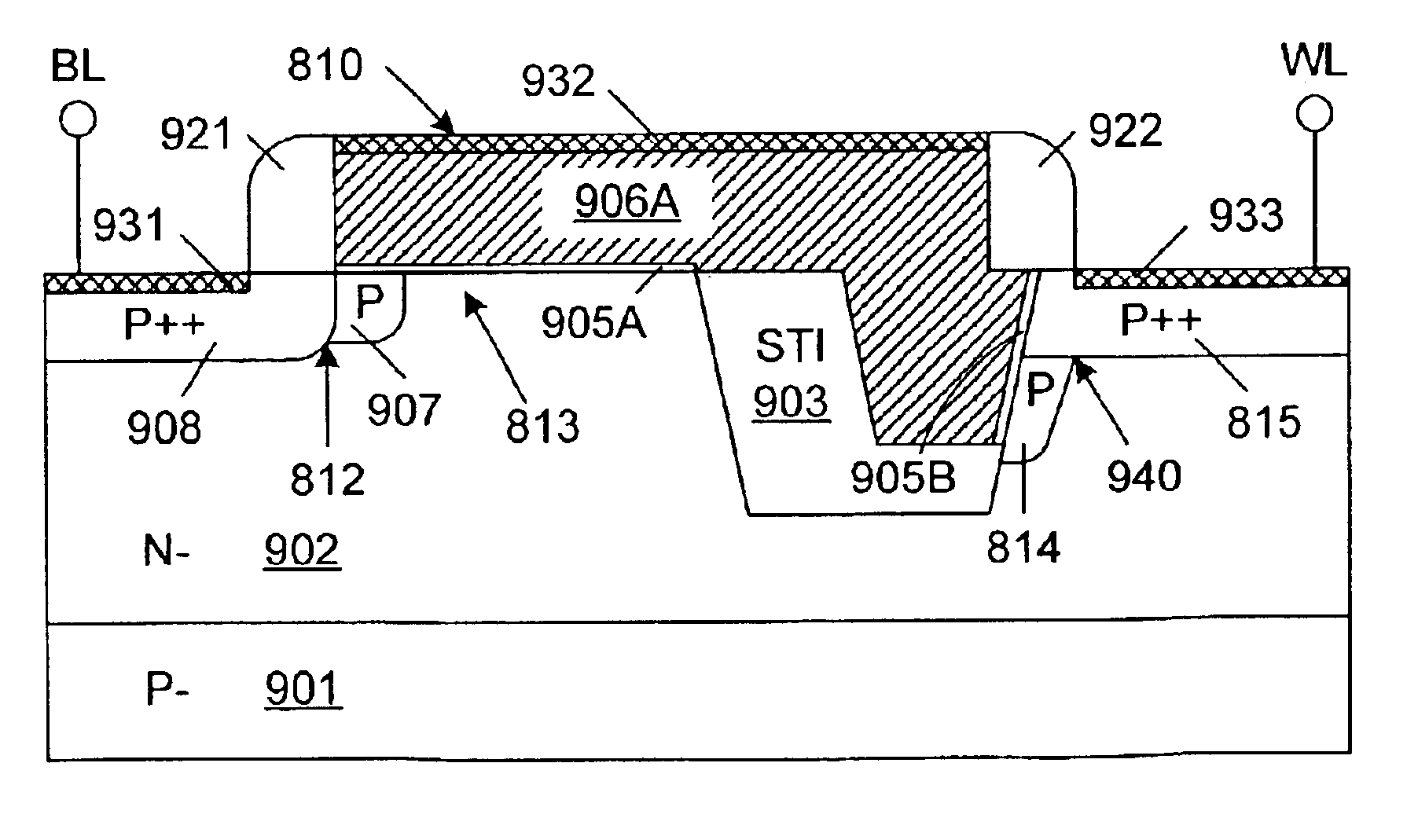
A non-volatile memory cell is fabricated using a conventional logic process, with minor modifications. The cell is fabricated by forming a shallow trench isolation (STI) region in a well region of a semiconductor substrate. A recessed region is formed in the STI region, wherein the recessed region extends into the STI region and exposes a sidewall region in the well region. A capacitor region is formed in the sidewall region. A dielectric layer is formed over the well region, including the sidewall region. A gate electrode is then formed over the dielectric layer, wherein a portion of the gate electrode extends into the recessed region. An access transistor of the cell is then formed in a self-aligned manner with respect to the gate electrode. A capacitor structure is formed by the gate electrode (in the recessed region), the dielectric layer on the sidewall region, and the capacitor region.

Description

FIELD OF THE INVENTIONThe present invention relates to non-volatile memory (NVM). More particularly, this invention relates to non-volatile memory cells fabricated by slightly modifying an application specific integrated circuit (ASIC) or conventional logic process. In the present application, a conventional logic process is defined as a semiconductor process that implements single-well or twin-well technology and uses a single layer of polysilicon. This invention further relates to a method of operating a non-volatile memory to ensure maximum data retention time.BACKGROUND OF INVENTIONFor system-on-chip (SOC) applications, it is desirable to integrate many functional blocks into a single integrated circuit. The most commonly used blocks include a microprocessor or micro-controller, static random access memory (SRAM) blocks, non-volatile memory blocks, and various special function logic blocks. However, traditional nonvolatile memory processes, which typically use stacked gate or sp...

Claims


Application Information

Patent Timeline
Patent Type & Authority Patents(United States)
IPC IPC(8): G11C7/20G11C7/00H01L21/02H01L21/28H01L21/70H01L21/336H01L21/8247G11C16/04H10B12/00
CPCG11C7/20H01L29/66825H01L27/11521H01L27/11558H01L21/28273G11C16/0416G11C2216/10H01L29/40114H10B41/60H10B41/30
Inventor HSU, FU-CHIEH
Owner MOSYS INC
Learn More