Reducing aberration in optical systems comprising cubic crystalline optical elements

a technology of optical elements and aberration, applied in the field of reducing aberration in optical systems, can solve the problems of reducing image resolution, introducing field distortion, and high cost of crytallographic orientations, and achieve the effect of reducing retardance in optical lithography systems

Inactive Publication Date: 2005-01-18
ASML NETHERLANDS BV
View PDF43 Cites 50 Cited by
  • Summary
  • Abstract
  • Description
  • Claims
  • Application Information

AI Technical Summary

Benefits of technology

[0017]In another aspect of the invention, an optical apparatus having an output comprises a plurality of optical elements divided into first and second sections and polarization conversion optics disposed between the first and second optical sections. The first and second sections have associated therewith polarization aberrations originating from variation in optical properties of the respective sections with polarization. The polarization aberrations affect the output of the optical apparatus. The polarization aberrations associated with the first section are substantially similar to the polarization aberrations associated with the second section. The polarization conversion optics are configured to transform an input polarization into a orthogonal output polarization such that the polarization aberrations associated with the first section at least partially offset the polarization aberrations associated with the second section. The effects of polarization aberrations on the output of the optical system are thereby reduced.
[0033]Yet another aspect of the invention comprises a method for reducing retardance in an optical beam propagating across an optical path through an optical system comprising one or more cubic crystal lens elements aligned along a common optical axis. The method comprises replacing one of the cubic crystal lens elements having a first optical power with two or more cubic crystal optical elements. The two or more cubic crystal optical elements together have a second optical power substantially matching the first optical power. The two or more cubic crystal optical elements may also comprise cubic crystal having crystal axes oriented differently. The two or more cubic crystal optical elements may comprise cubic crystal having different crystal axis substantially aligned along the common optical axis. One of the cubic crystal lens elements may be replaced with a [100] and a [110] cubic crystal element having respective [100] and [110] cubic crystal axes substantially aligned with the common optical axis. One of the cubic crystal lens elements may be replaced with a [111] and a [110] cubic crystal element having respective [111] and [110] cubic crystal axes substantially aligned with the common optical axis. Also, one of the cubic crystal lens elements may be replaced with a [100] and a [111] cubic crystal element having respective [100] and [111] cubic crystal axes substantially aligned with the common optical axis. In some embodiments, the two or more cubic crystal optical elements may comprise cubic crystal having substantially the same crystal axis substantially aligned along the common optical axis, and the method may further comprise rotating said optical elements about the optical axis to an orientation that reduces retardance in said optical beam. One of the cubic crystal lens elements may be replaced with two [111] cubic crystal lens elements having respective [111] cubic crystal axes substantially aligned with the common optical axis. Also, in various embodiments, the method may further comprise inserting polarization rotation optics in the optical path to rotate the polarization of the beam and to reduce beam retardance.

Problems solved by technology

These crystals, however, are expensive, and certain orientations, such as the and crytallographic orientations are more expensive than others, like the crystal orientation.
When used for construction of elements of an optical system, the birefringent properties of these cubic crystalline materials may produce wavefront aberrations that significantly degrade image resolution and introduce field distortion.
These aberrations are particularly challenging for optical instruments employed in photolithography in today's semiconductor manufacturing industry where high resolution and tight overlay requirements are demanded by an emphasis on increased levels of integration and reduced feature sizes.
Strong intrinsic birefringence at this wavelength has the unfortunate effect of producing wavefront aberrations that can significantly degrade image resolution and introduce distortion of the image field, particularly for sub-micron projection lithography in semiconductor manufacturing.

Method used


Image

  • Reducing aberration in optical systems comprising cubic crystalline optical elements
  • Reducing aberration in optical systems comprising cubic crystalline optical elements
  • Reducing aberration in optical systems comprising cubic crystalline optical elements

Examples


example 1

[0132]FIG. 6 shows an exemplary optical system 160 usable for lithographic applications that is based on a Dyson catadioptric lens comprising a single refractive element 162 and single reflective element 164 aligned along an optical axis 165 [Refs. J. Dyson, “Unit magnification optical system without Seidel aberrations,” J. Opt. Soc. Am., Vol. 49, p. 713 (1959), as described in R. Kingslake, Lens Design Fundamentals, Academic Press, Inc. (1978)] In one preferred embodiment, the refractive optical element comprises cubic crystalline material. This refractive element 162 has first planar surface 166 and second curved surface 168. The reflective element 164 also has a curved reflective surface 170.

[0133]A notable feature of the Dyson design is that the object and image fields 172, 174 are coplanar and located at the center of curvature, C, of the curved surfaces on the refractive and reflective elements 160 and 162. Preferably, the radius of curvature, R1, of the refractive element 162...

example 2

[0157]A mixing rod, also referred to as a homogenizer or kaleidoscope, is commonly used in illumination systems for photolithography. FIG. 12 shows an exemplary mixing rod 200 comprising calcium fluoride and having dimensions of 10×10×160 millimeters (mm). The mixing rod 200 is assumed to have a birefringence magnitude, ne−no, of −12×10−7 corresponding to the intrinsic birefringence of calcium fluoride measured at a wavelength of 157 nanometers (nm) as suggested in D. Krahmer, “Intrinsic Birefringence in CaF2,” at Calcium Fluoride Birefringence Workshop, Intl. SEMATECH, Jul. 31, 2001. The mixing rod 200 has proximal and distal ends 202, 204 and an input and output faces or ports 206, 208 for inputting and outputting the beam and walls 210 on opposite sides for reflecting the beam propagating therethrough. An optical axis 212 extends the length of the mixing rod 200. The mixing rod 200 can be separated into two portions 214, 216, preferably of equal length, and more preferably having...

example 3

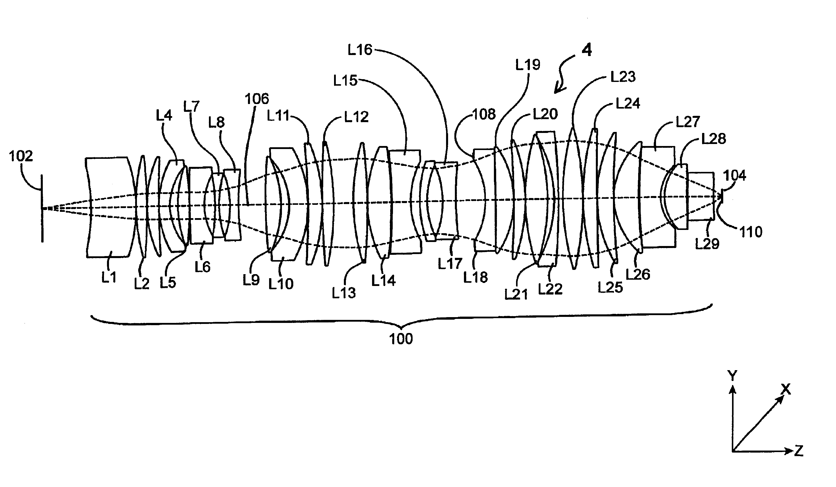
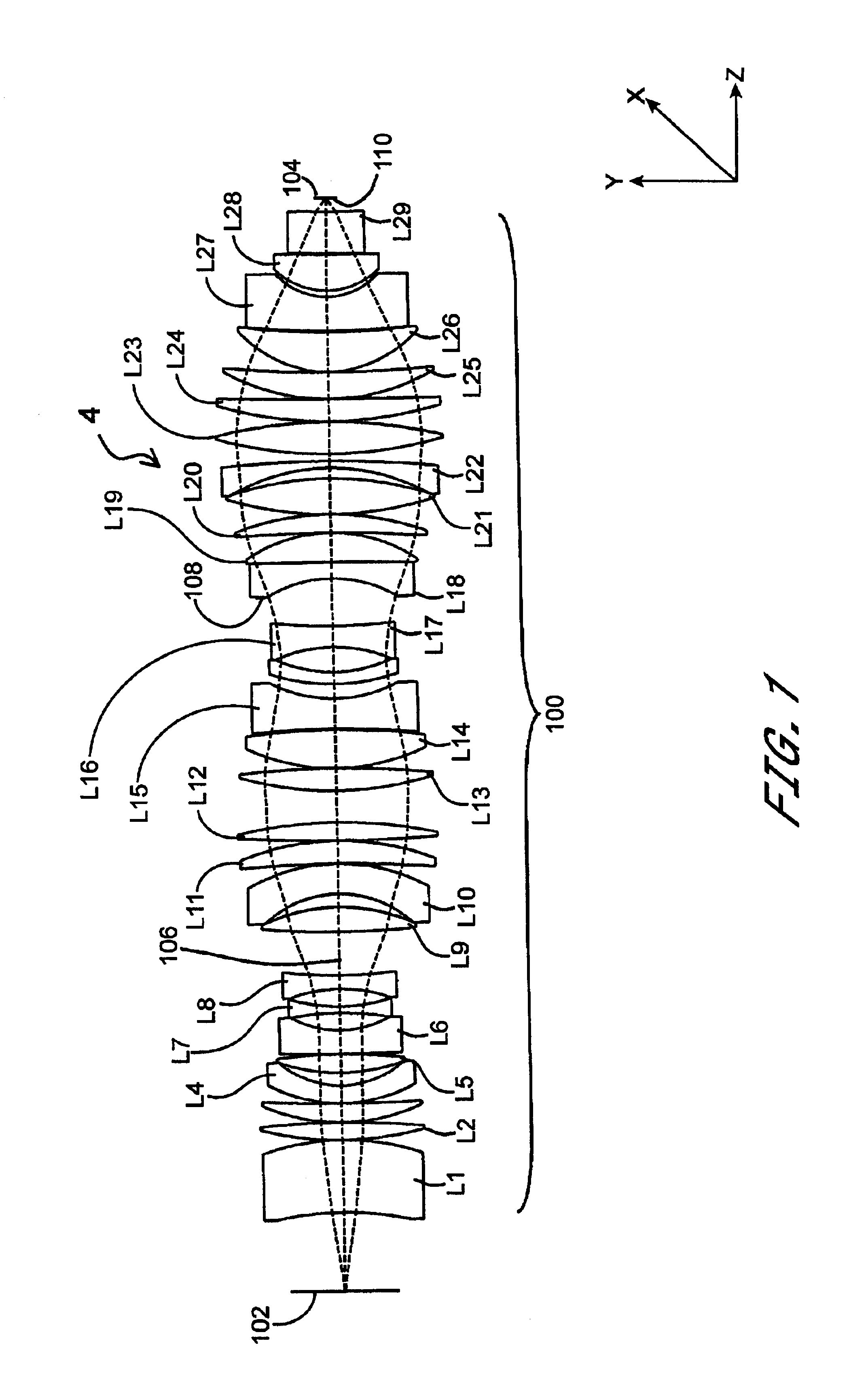
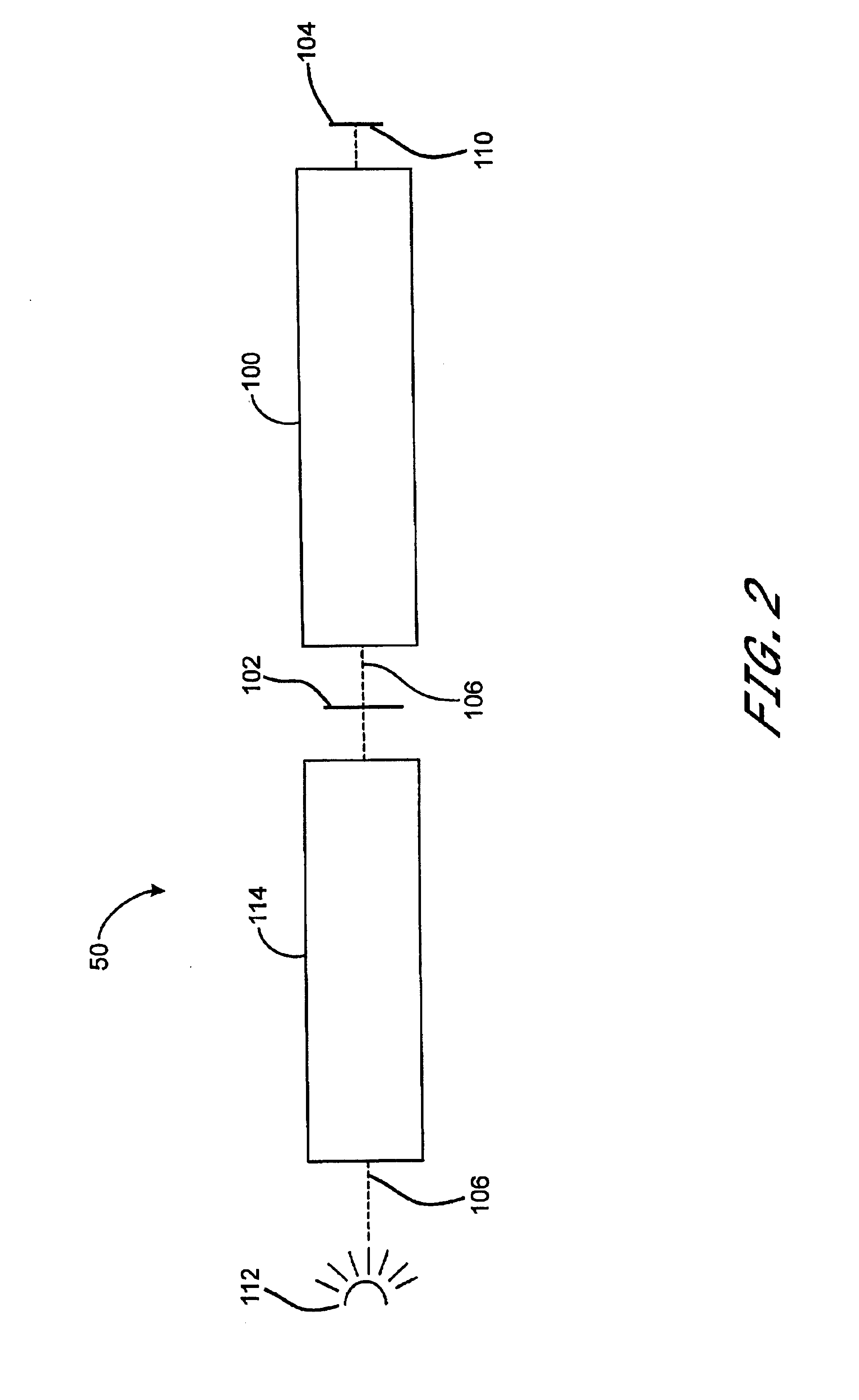
[0170]These techniques for reducing polarization aberrations caused by intrinsic birefringence are particularly well suited for providing wavefront correction of refractive imaging systems used for photolithography. In addition to the rigorous performance requirements associated with this application, photolithography lenses often include a large number of refractive optical elements, which together possess a significant amount of birefringence. Wavefront error caused by retardation aberrations can therefore substantially limit the resultant resolution obtained by the photolithographic projection system. An exemplary projection lens 100, one which contains all optically transmissive and, in particular, all refractive, powered, optical elements L1-L29 is illustrated in FIG. 1. A similar lens is provided in European Patent Application No. 0 828 172 by S. Kudo and Y. Suenaga, the contents of which are herein incorporated by reference. This optical system 100 is designed to operate at a...


PUM

PropertyMeasurementUnit
wavelengthaaaaaaaaaa
optical wavelengthaaaaaaaaaa

Abstract

An optical system includes multiple cubic crystalline optical elements and one or more polarization rotators in which the crystal lattices of the cubic crystalline optical elements are oriented with respect to each other to reduce the effects of intrinsic birefringence and produce a system with reduced retardance. The optical system may be a refractive or catadioptric system having a high numerical aperture and using light with a wavelength at or below 248 nanometers. The net retardance of the system is less than the sum of the retardance contributions of the respective optical elements. In one embodiment, all cubic crystalline optical elements are oriented with identical three dimensional cubic crystalline lattice directions, a 90° polarization rotator divides the system into front and rear groups such that the net retardance of the front group is balanced by the net retardance of the rear group. The optical system may be used in a photolithography tool to pattern substrates such as semiconductor substrates and thereby produce semiconductor devices.

Description

PRIORITY APPLICATION[0002]This application claims the benefit of priority under 35 U.S.C. §119(e) to U.S. Provisional Patent Application No. 60 / 385,427, filed May 31, 2002 and entitled “Structures and Methods for Reducing Aberrations in Optical Systems”, U.S. Provisional Patent Application No. 60 / 367,911, filed Mar. 26, 2002 and entitled “Structure and Method for Improving Optical Systems”, U.S. Provisional Patent Application No. 60 / 363,808, filed Mar. 12, 2002, and entitled “Correction of Intrinsic Birefringence Using Rotators”, U.S. Provisional Patent Application No. 60 / 332,183, filed Nov. 21, 2001, and entitled “Compensation for Intrinsic Birefringence Effects in Cubic Crystalline Optical Systems” as well as U.S. Provisional Patent Application No. 60 / 335,093, filed Oct. 30, 2001, and entitled “Intrinsic Birefringence Compensation”, which are each hereby incorporated by reference herein in their entirety.BACKGROUND OF THE INVENTION[0003]1. Field of the Invention[0004]The present i...

Claims


Application Information

Patent Timeline
Patent Type & Authority Patents(United States)
IPC IPC(8): G03F7/20G02B27/28
CPCG02B1/08G02B5/3083G02B13/22G03F7/70966G03F7/70075G03F7/70216G02B27/28
Inventor MCGUIRE, JR., JAMES P.
Owner ASML NETHERLANDS BV
Why Eureka
Try Eureka