Semiconductor device and method of manufacturing the same

a semiconductor and semiconductor technology, applied in vacuum evaporation coatings, chemical vapor deposition coatings, coatings, etc., can solve the problems of increased leakage current flowing from the gate metal to the substrate via the siosub>2 /sub>layer, serious problem, and high-k dielectric materials

Active Publication Date: 2005-02-01
KIOXIA CORP
View PDF1 Cites 16 Cited by
  • Summary
  • Abstract
  • Description
  • Claims
  • Application Information

AI Technical Summary

Benefits of technology

A second aspect of the present invention proposes a method of manufacturing a semiconductor device including a metal silicate layer formed on a semiconductor substrate, the metal silicate layer containing at least nitrogen and including a first layer region located at a side of the semiconductor substrate, a second layer region located at a side opposite to that of the first layer region, and a third layer region located between the first and second layer regions, the method including: depositing a metal silicate layer having a uniform metal concentration throughout the first, second, and third layer regions; and performing a heat treatment on the metal silicate layer so that a nitrogen concentration in the metal silicate layer becomes higher in the third layer region than in the first and second layer regions.

Problems solved by technology

However, when the thickness of the SiO2 layer is decreased to be as thin as 1 nm, a problem arises in that there is an increase in a leakage current flowing from a gate metal to a substrate via the SiO2 layer.
In particular, this problem is serious in a MISFET with a low standby power.
However, there is a problem in that a high-k dielectric material tends to generate an interface state, a fixed charge, etc., because generally a high-k dielectric material does not have a good interface characteristic at an interface with a silicon substrate.
However, a metal silicate is superior in interface characteristic at an interface with a silicon wafer, resulting in that a decrease in drive current capability caused by interface defects, which is easy to occur in the case of a general high-k material, is unlikely to occur.
For example, when a metal silicate is used to form a gate dielectric film of an FET, there is a problem in that electrons flowing through a channel region at a surface of the silicon substrate suffer the influence of remote scattering caused by a potential field generated by the metal contained in the metal silicate.
Furthermore, nitrogen added to the metal silicate is also considered to be a cause of the degradation of the interface characteristic.
However, since the metal or nitrogen concentration at the gate electrode side is higher in the aforementioned structures, the band offset of the dielectric film decreases, which may result in an increase in leakage current.

Method used


Image

  • Semiconductor device and method of manufacturing the same
  • Semiconductor device and method of manufacturing the same
  • Semiconductor device and method of manufacturing the same

Examples


first embodiment

(First Embodiment)

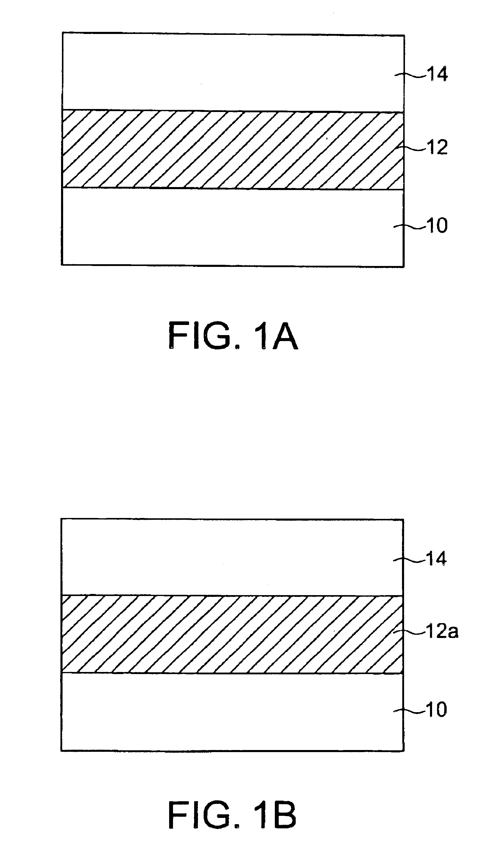
FIGS. 1A and 1B are sectional views for explaining a method of manufacturing a MISFET according to a first embodiment of the present invention, and a semiconductor device obtained thereby.

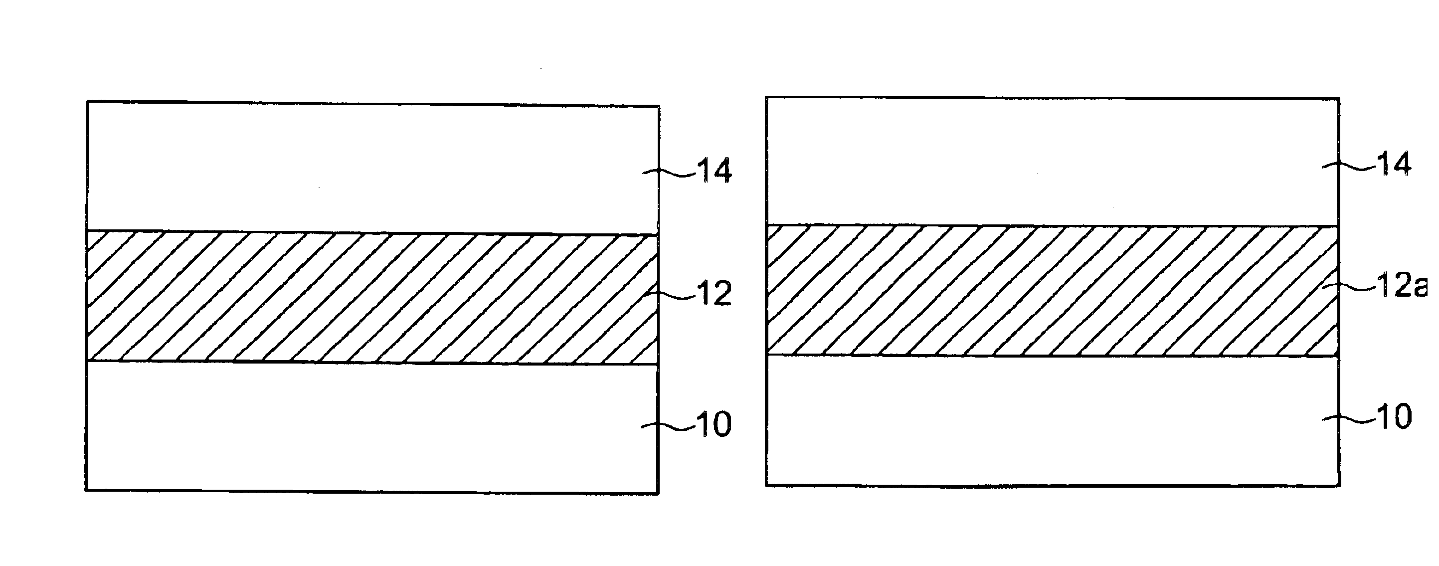
First, as shown in FIG. 1A, a zirconium silicate layer 12, to which nitrogen is doped, is formed on a semiconductor substrate, e.g., a silicon substrate 10, followed by a cap layer 14. The nitrogen-doped zirconium silicate layer 12 is formed of a nitrogen-doped zirconium-silicon compound, and has substantially uniform composition distributions of zirconium and silicon in a depth direction of the layer. The depth direction of the zirconium silicate layer 12 herein means a direction extending from the interface with the cap layer 14 to the interface with the silicon substrate 10.

The cap layer 14 is formed of, e.g., a conductive material such as an impurity-doped polycrystalline silicon.

The composition distributions of the elements in the zirconium silicate layer 12 at this stage wil...

second embodiment

(Second Embodiment)

A method of manufacturing a gate dielectric film of a MISFET according to a second embodiment of the present invention will be described below. FIGS. 5A to 5C are sectional views showing the steps of manufacturing the MISFET of the second embodiment.

First, a semiconductor substrate, e.g., a silicon substrate 10, is prepared, on which element isolation regions (not shown in the drawings) for electrically isolate adjacent devices are formed. Then, a native oxide layer on the surface of the silicon substrate 10 is removed with diluted hydrofluoric (HF) acid solution, and dangling bonds at the surface of the silicon substrate 10 are hydrogen-terminated. Then, a metal silicate layer 12 with a uniform composition is formed on the silicon substrate 10 (FIG. 5A). A zirconium silicate layer having a thickness of 2 nm is an example of such a metal silicate layer. In this case, a zirconium oxide target and a silicon oxide target are used, and sputtering is performed using mi...

third embodiment

(Third Embodiment)

Next, a semiconductor device according to a third embodiment of the present invention will be described with reference to FIGS. 7, 8A, 8B, and 8C. Generally, not only a metal silicate, but also a metal oxide without positively containing silicon can be used as a material of a dielectric film. In the third embodiment, a gate dielectric film formed of such a metal oxide will be described.

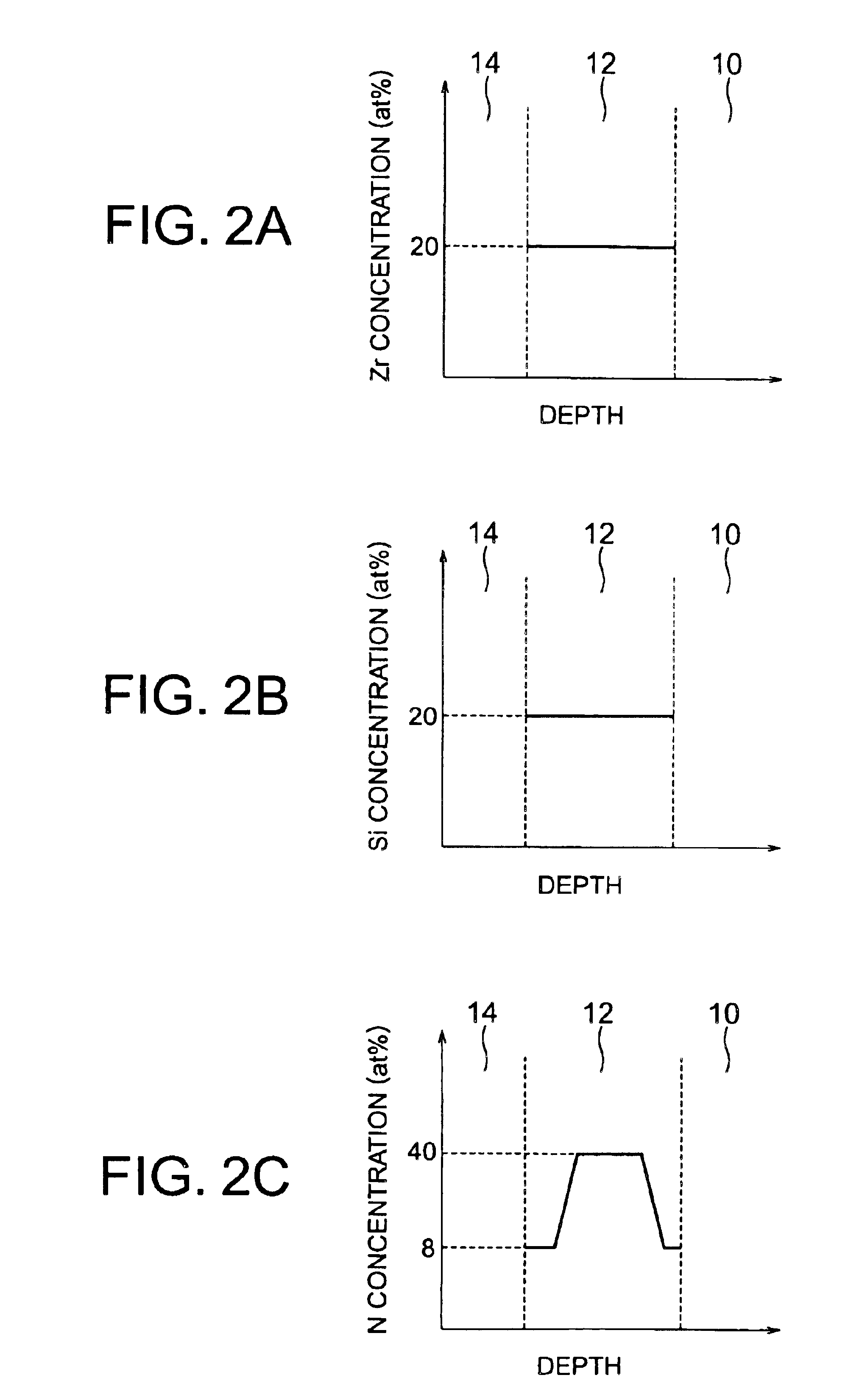
FIG. 7 is a sectional view of a laminated structure obtained by first forming a metal oxide layer 34 on a silicon substrate 10, and then forming a conductive cap layer 14 on the metal oxide layer 34. FIGS. 8A, 8B, and 8C schematically show concentration distributions of a metal (e.g., Zr), nitrogen (N), and oxygen (O) in the metal oxide layer 34.

As can be understood from FIG. 8A, the metal concentration in the depth direction in the metal oxide layer 34 is uniform. This means herein that the variations in concentrations are in the range of about 20 % or less.

As can be understood from...


PUM

PropertyMeasurementUnit
thicknessaaaaaaaaaa
relative dielectric constantaaaaaaaaaa
temperatureaaaaaaaaaa

Abstract

A good interface characteristic can be maintained, and a leakage current of a dielectric film can be decreased. A semiconductor device according to one aspect of the present invention includes: a semiconductor substrate; a gate dielectric film containing at least nitrogen and a metal, the gate dielectric film being formed on the semiconductor substrate, and including a first layer region contacting the semiconductor substrate, a second layer region located at a side opposite to that of the first layer region in the gate dielectric film, and a third layer region located between the first and second layer regions, a maximum value of a nitrogen concentration in the third layer region being higher than maximum values thereof in the first and second layer regions; a gate electrode contacting the second layer region; and a pair of source and drain regions formed at both sides of the gate dielectric film in the semiconductor substrate.

Description

CROSS-REFERENCE TO RELATED APPLICATIONSThis application is based upon and claims the benefit of priority from prior Japanese Patent Application No. 2003-48515, filed on Feb. 26, 2003 in Japan, the entire contents of which are incorporated herein by reference.BACKGROUND OF THE INVENTION1. Field of the InventionThe present invention relates to a semiconductor device having a MIS (Metal-Insulator-Semiconductor) structure, to which an electric field is applied, such as a field effect transistor, and a method of manufacturing such a semiconductor device.2. Related ArtIn order to meet the requirements of a speed-up and a higher integration of LSIs, the miniaturization of transistors is being further advanced. As this trend is accelerating, a thinner gate dielectric film is continuously being sought after. In a conventional field effect transistor having a MIS structure (MISFET=Metal-Insulator-Semiconductor Field Effect Transistor), SiO2 is used as a material of a gate dielectric film. How...

Claims


Application Information

Patent Timeline
Patent Type & Authority Patents(United States)
IPC IPC(8): H01L21/02H01L21/28H01L29/40H01L29/51C23C14/06C23C16/30H01L21/316H01L29/78
CPCH01L21/28185H01L29/518H01L29/513H01L21/28202H01L21/28194H01L29/517H01L21/02329H01L29/41725H01L29/42312H01L29/4232H01L29/66477
Inventor HIRANO, IZUMIKOYAMA, MASATONISHIYAMA, AKIRA
Owner KIOXIA CORP
Why Eureka
Try Eureka