Trench isolation for semiconductor devices

a technology of semiconductor devices and trenches, applied in the direction of solid-state devices, transistors, radio-controlled devices, etc., can solve the problems of high current leakage, current leakage can occur at the junction between active device regions and trenches, and the problem of parasitic inter-device current becomes more problematic, so as to improve electrical isolation and reduce optical cross-talk

Inactive Publication Date: 2005-02-15
MICRON TECH INC
View PDF14 Cites 38 Cited by
  • Summary
  • Abstract
  • Description
  • Claims
  • Application Information

AI Technical Summary

Benefits of technology

In some implementations, shallow ion implants are provided to establish field threshold voltage implants to improve the electrical isolation between active areas. Deep implants can be provided, for example, to reduce the optical cross-talk between adjacent photosensitive pixels in CMOS or CCD imagers.

Problems solved by technology

As the density of the devices continues to rise, parasitic inter-device currents become more problematic.
841-844 (1996), some ion implants can result in high current leakage.
In particular, when ions are implanted in the substrate close to the edges of the trench, current leakage can occur at the junction between the active device regions and the trench.
Similarly, if the trench is shallow, then a photon impinging on a particular pixel of a photosensitive device may diffuse under the trench isolation structure to an adjacent pixel, resulting in detection of the photon by the wrong-pixel.

Method used


Image

  • Trench isolation for semiconductor devices
  • Trench isolation for semiconductor devices
  • Trench isolation for semiconductor devices

Examples


Embodiment Construction

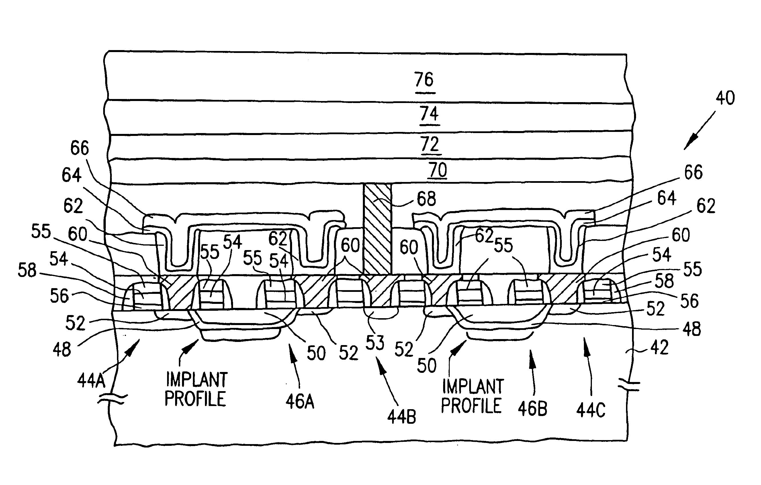
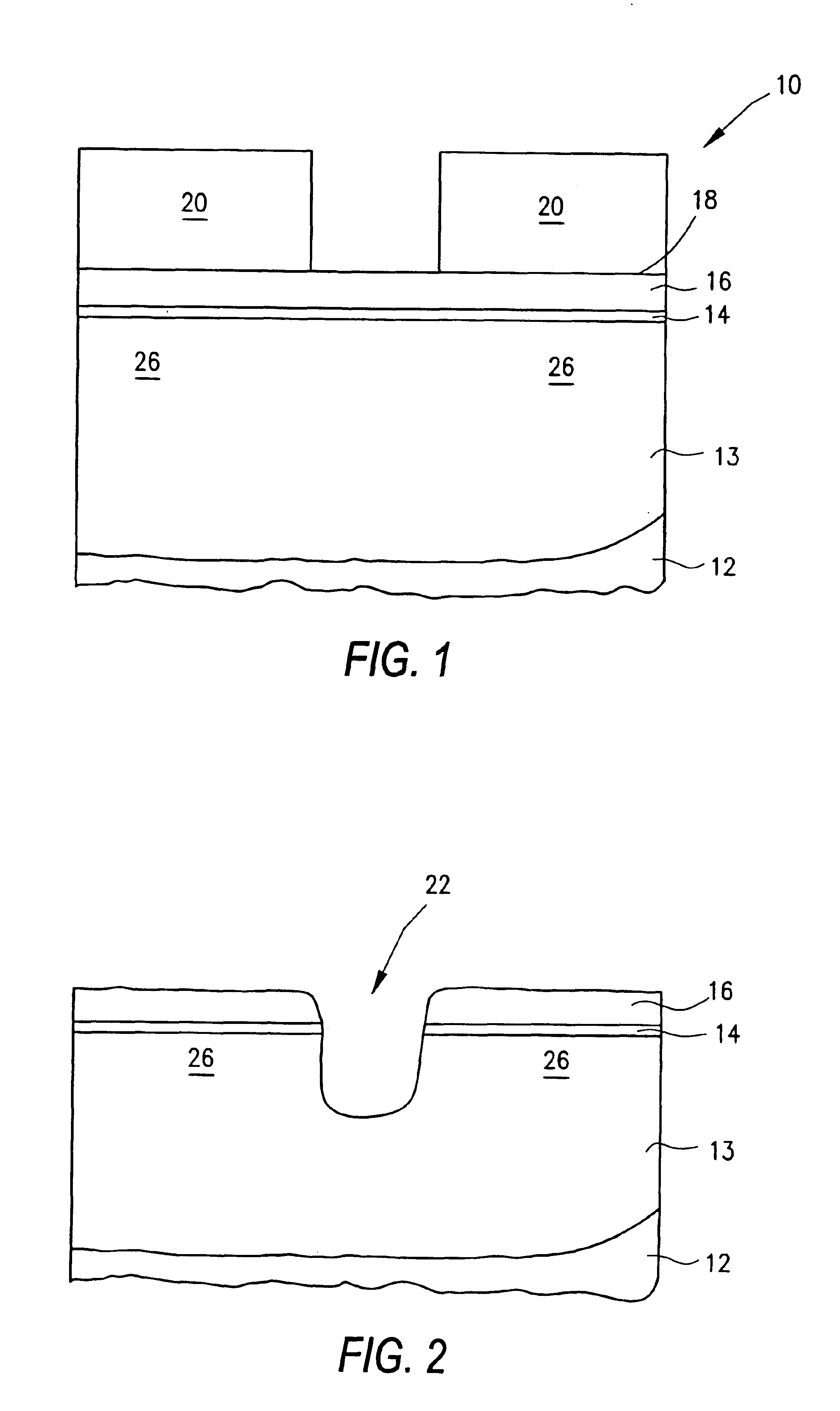
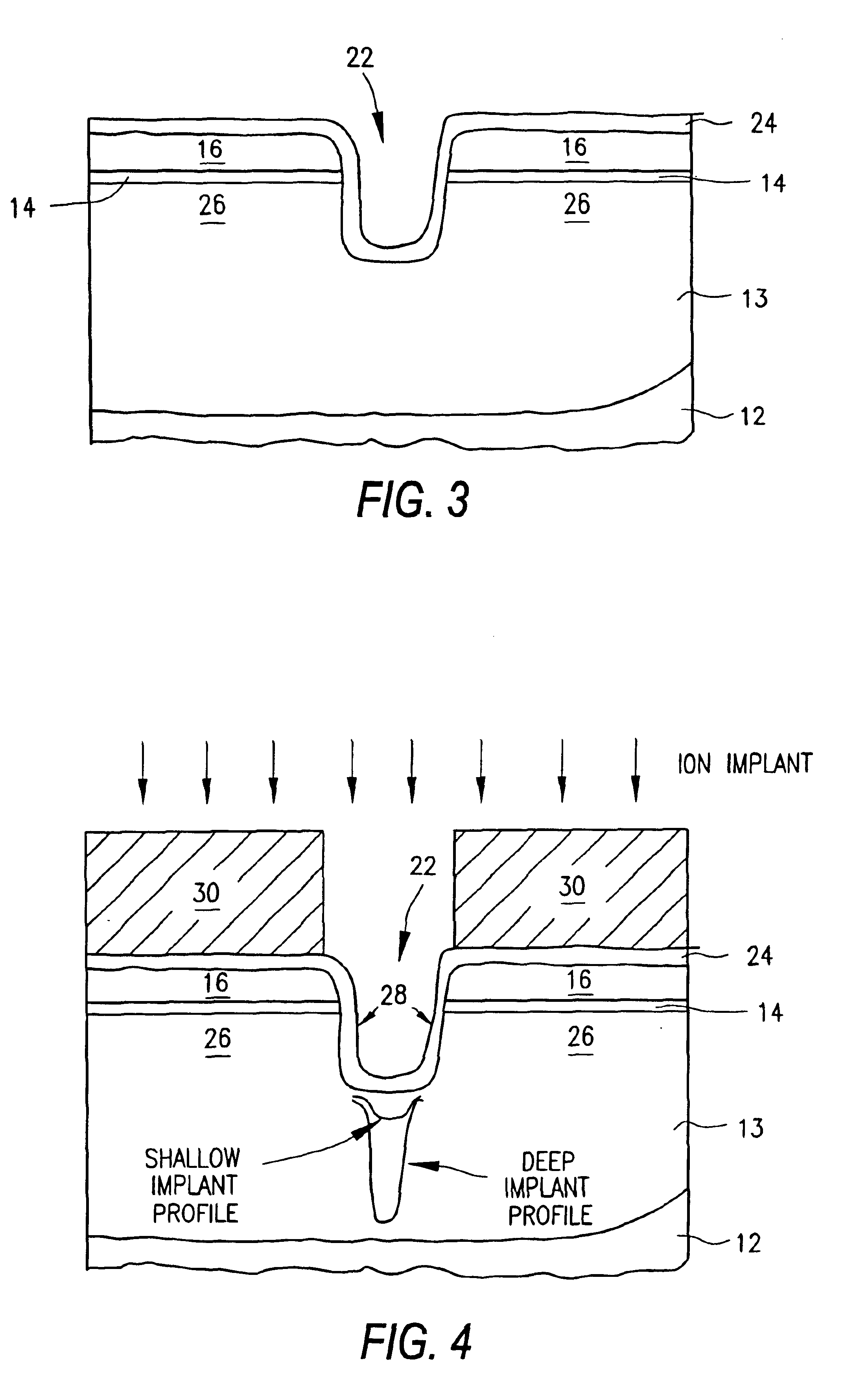
Referring to FIG. 1, a silicon or other semiconductor wafer 10 includes a bulk substrate region 12. Typically, ions are implanted in the substrate 12 to form n-type wells and p-type wells which define the locations of the n-channel and p-channel devices 26. For example, the substrate 12 can be implanted with a p-type dopant such as boron (B) to form a p-well 13. For ease of illustration, the figures show active areas and STI field isolation regions in a single well type. However, in general, the invention is applicable to other semiconductor device isolation regions such as n-well and p-well regions in p-type substrates, n-type substrates and epitaxial substrates, including p on p+, p on p−, n on n+, and n on n−. In some implementations, the substrate 12 can comprise gallium arsenide (GaAs) or other semiconductor materials such as InP, CdS, CdTe and the like.

A layer of pad oxide 14 is provided atop the substrate 12, for example, either by deposition or by oxidizing conditions. A sac...


PUM


Abstract

A method of fabricating an integrated circuit includes forming an isolation trench in a semiconductor substrate and partially filling the trench with a dielectric material so that at least the sidewalls of the trench are coated with the dielectric material. Ions are implanted into the substrate in regions directly below the isolation trench after partially filling the trench with the dielectric material. The dielectric along the sidewalls of the trenches can serve as a mask so that substantially all of the ions implanted below the isolation trenches are displaced from the active regions. The dielectric along the sidewalls of the trenches serves as a mask so that substantially all of the ions implanted below the isolation trenches are displaced from the active regions. After the ions are implanted in the substrate below the trenches, the remainder of the trench can be filled with the same or another dielectric material. The trench isolation technique can be used to fabricate memory, logic and imager devices which can exhibit reduced current leakage and/or reduced optical cross-talk.

Description

BACKGROUNDThe present invention relates generally to semiconductor devices and, more particularly, to trench isolation process technology for use in memory, image, logic and other semiconductor devices.Implementing electronic circuits involves connecting isolated devices or circuit components through specific electronic paths. In silicon integrated circuit (IC) fabrication, it is necessary to isolate devices that are formed in a single substrate from one another. The individual devices or circuit components subsequently are interconnected to create a specific circuit configuration.As the density of the devices continues to rise, parasitic inter-device currents become more problematic. Isolation technology, therefore, has become a critical aspect of integrated circuit fabrication.For example, dynamic random access memory (DRAM) devices generally comprise an array of memory cells for storing data and peripheral circuits for controlling data in the memory cells. Each memory cell in a D...

Claims


Application Information

Patent Timeline
Patent Type & Authority Patents(United States)
IPC IPC(8): H01L21/70H01L21/762
CPCH01L21/76237H01L27/14689H01L27/1463H01L27/14643
Inventor RHODES, HOWARD E.
Owner MICRON TECH INC
Why Eureka
Try Eureka