

Method of manufacturing semiconductor device
a manufacturing method and semiconductor technology, applied in the direction of semiconductor devices, electrical devices, transistors, etc., can solve the problems of reducing the processing time, affecting the quality of the product, so as to reduce the number of heat treatments, enhance the through-put, and simplify the process
- Summary
- Abstract
- Description
- Claims
- Application Information
AI Technical Summary
Benefits of technology
Problems solved by technology
Method used
Image

Examples
embodiments
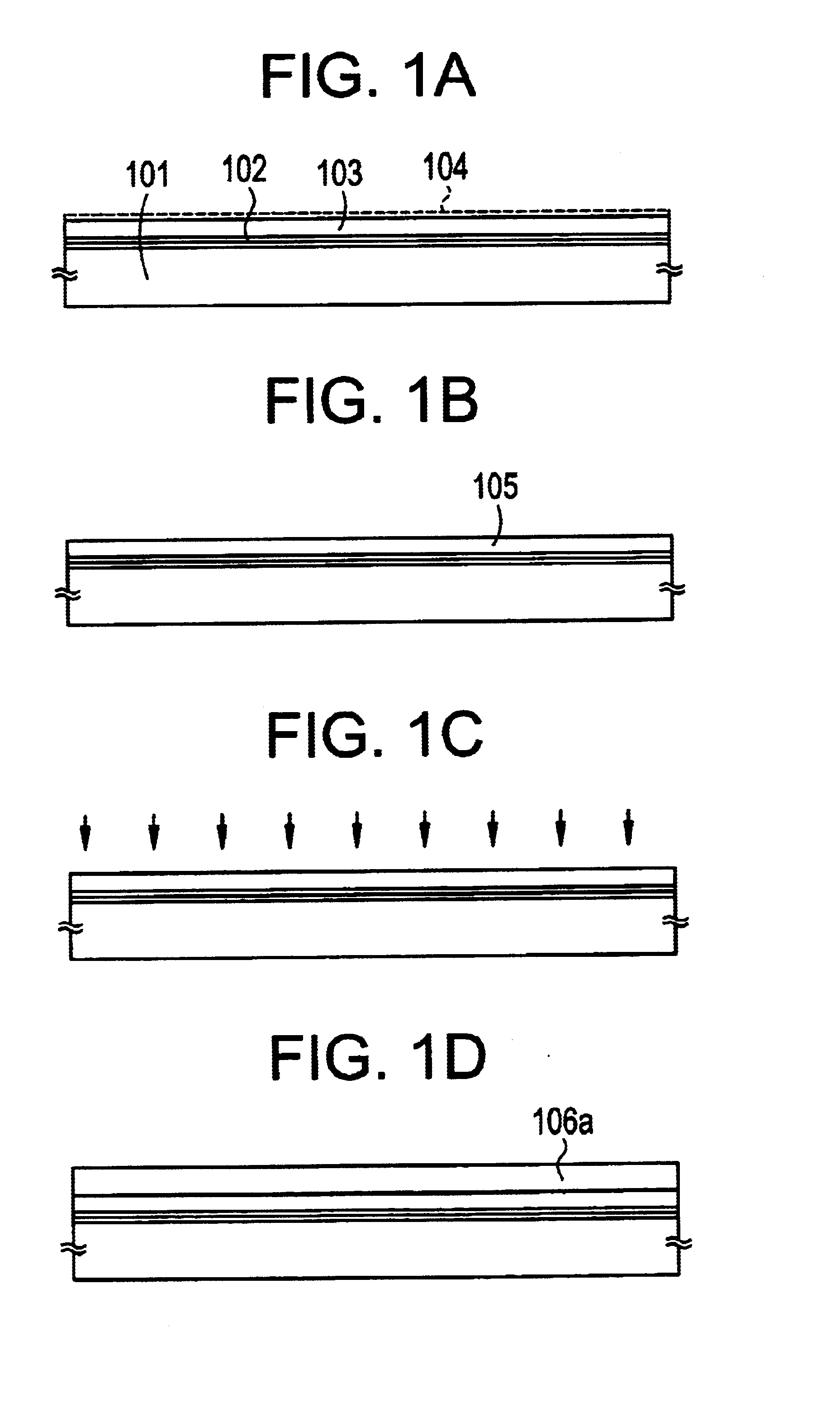
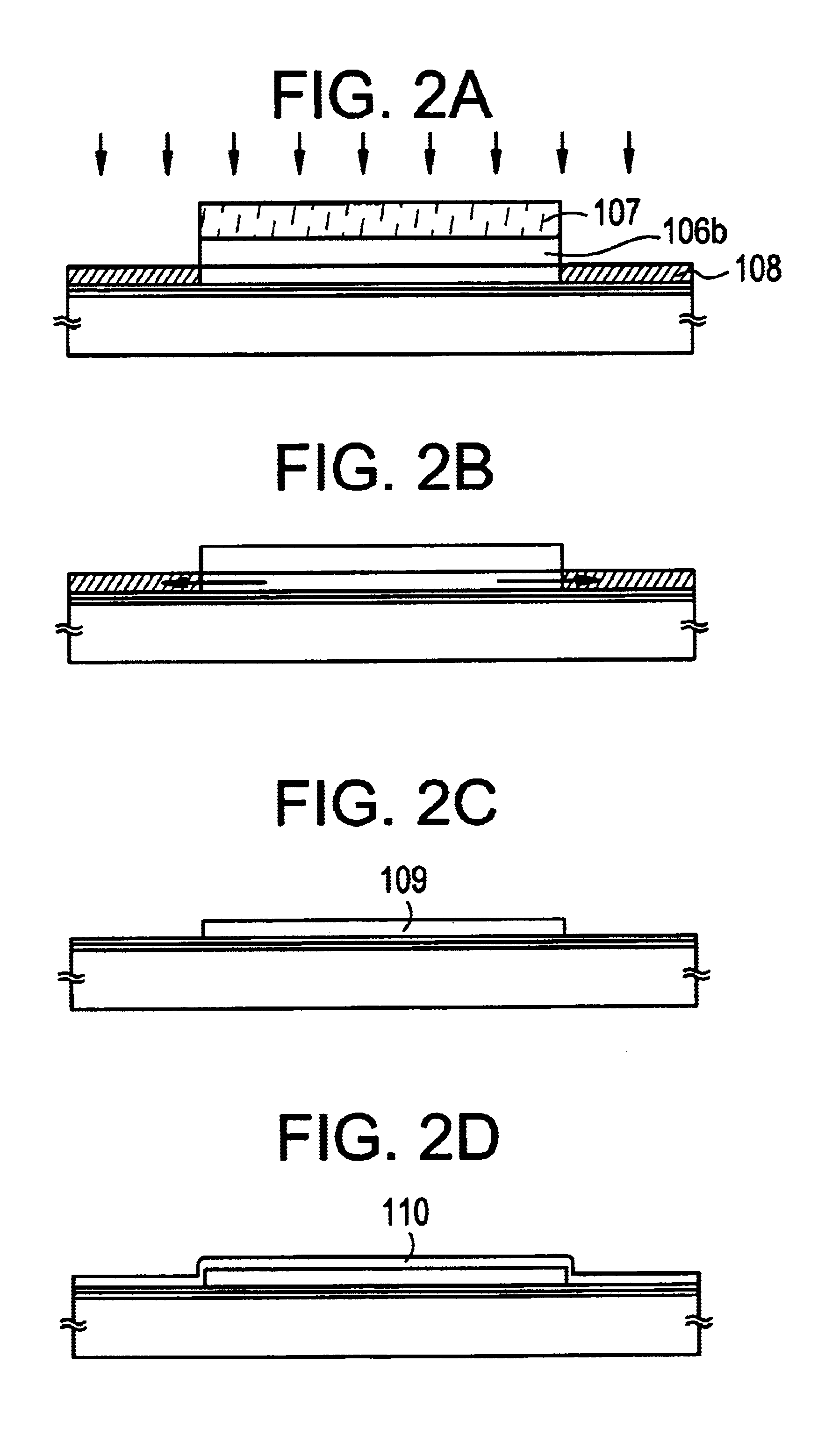
[Embodiment 1]
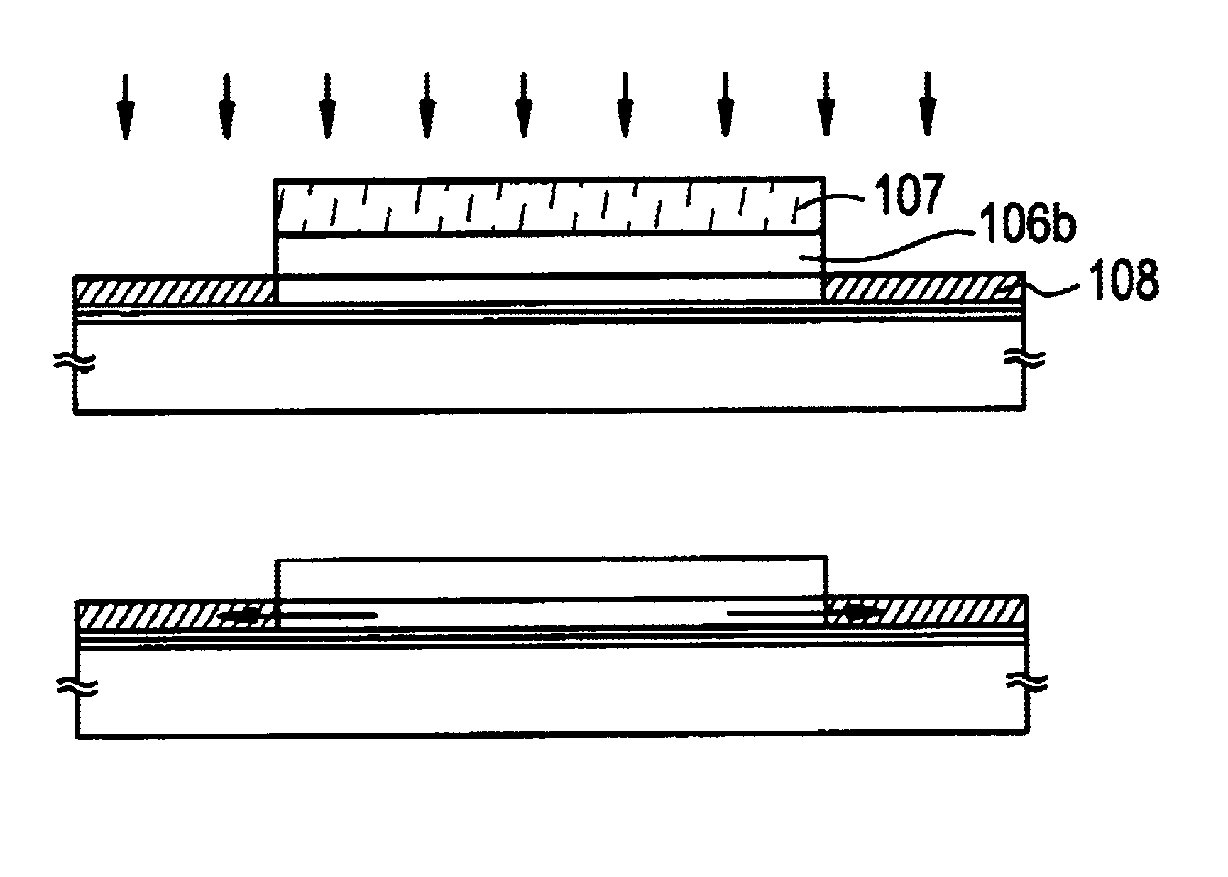
Herein, a method of simultaneously manufacturing a pixel portion and TFTs (an n-channel TFT and a p-channel TFT) of a driving circuit provided on the periphery of the pixel portion on the same substrate will be described with reference to FIGS. 3A-3C to 6.
First, in the present embodiment, a substrate 200 made of barium borosilicate glass such as #7059 and #1737 produced by Corning Co. or aluminoborosilicate glass is used. There is no particular limit to the substrate 200 as long as it has light transparency, and a quartz substrate may be used. Furthermore, a plastic substrate having heat resistance enduring a treatment temperature in the present embodiment may be used.
Then, a base film 201 composed of an insulating film such as a silicon oxide film, a silicon nitride film, or a silicon oxynitride film is formed on the substrate 200. In the present embodiment, the base film 201 has a two-layered structure; however, the base film 201 may be composed of a single-layer fil...
embodiment 2
[Embodiment 2]
In this embodiment, a process for manufacturing an active matrix liquid crystal display device using the active matrix substrate manufactured in embodiment 1 will be described. The description is made with reference to FIG. 6.
First, after the active matrix substrate with the state of FIG. 5 is obtained according to embodiment 1, an orientation film 401 is formed on the active matrix substrate of FIG. 5 to perform a rubbing process. Note that, in this embodiment before the formation of the orientation film 401, an organic resin film such as an acrylic resin film is patterned to form a columnar spacer for keeping a gap between substrates in a desired position. Also, instead of the columnar spacer, a spherical spacer may be distributed over the entire surface.
Next, an opposing substrate 400 is prepared. A color filter in which a colored layer 402 and a light shielding layer 403 are arranged corresponding to each pixel is provided in this opposing substrate 400. Also a lig...
embodiment 3
[Embodiment 3]
The present embodiment is different from Embodiment 1 in the process after formation of the insulating film 106a to be a mask. In the present embodiment, after a resist mask is removed, a rare gas element is added. The remaining processes are the same as those in Embodiment 1, so that the same reference numerals as those in FIGS. 2A to 2D are used in FIGS. 9A to 9D.
First, the same state as that in FIG. 1D is obtained in accordance with the embodiment. Then, a resist mask is formed in accordance with the embodiment, and a silicon oxide film is patterned to form a mask made of a silicon oxide film. After the resist mask is removed, a rare gas element is added (FIG. 9A).
If the remaining processes are conducted in accordance with Embodiment 3 states in FIGS. 9B to 9D are obtained. If the remaining processes are conducted in accordance with Embodiment 1, the active matrix substrate shown in FIG. 6 is obtained.
The present embodiment can be combined with Embodiment 2.
PUM
 Abstract
Description
Claims
Application Information