

Methods for fabricating group III nitride compound semiconductors and group III nitride compound semiconductor devices
- Summary
- Abstract
- Description
- Claims
- Application Information
AI Technical Summary
Benefits of technology
Problems solved by technology
Method used
Image

Examples
first embodiment
[0097][First Embodiment]
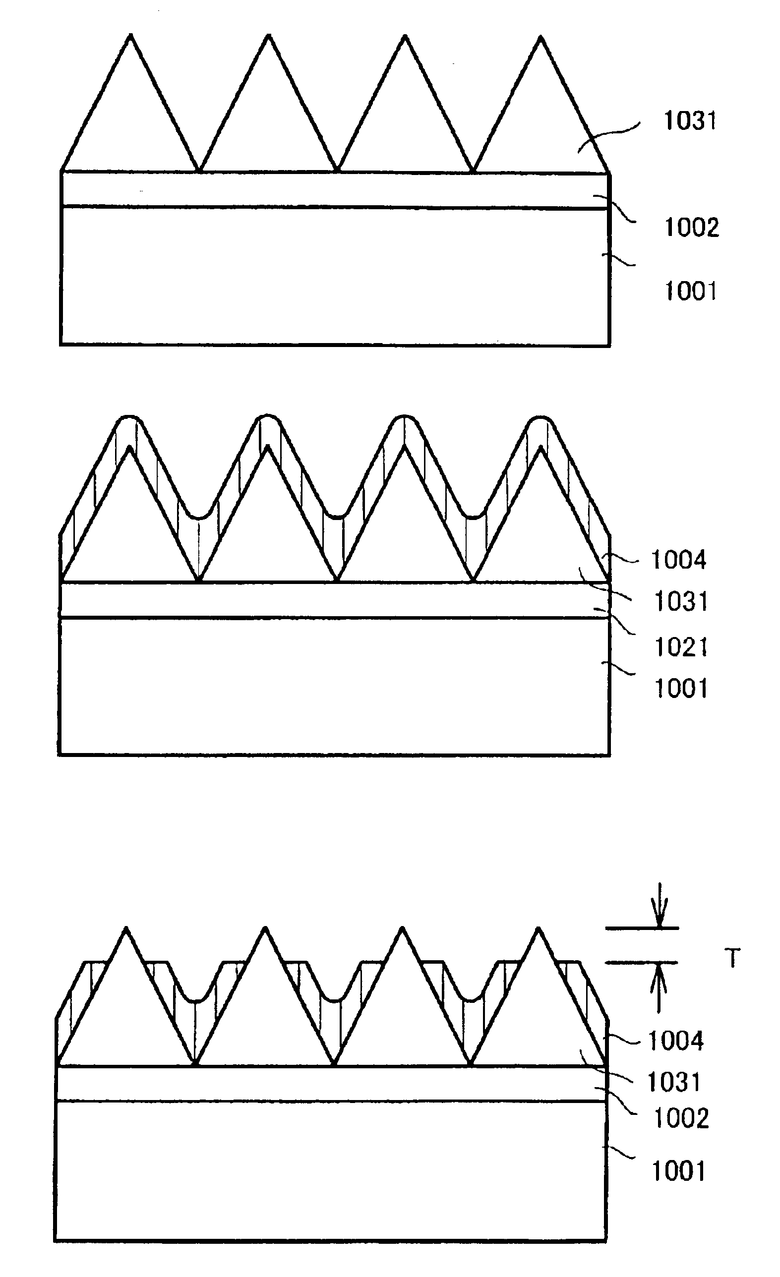
[0098]FIGS. 1 and 2 show the steps of the present embodiment. A monocrystalline sapphire substrate 1001 containing an a-plane as a primary crystal plane was cleaned through organic cleaning and heat treatment. The temperature of the substrate 1001 was lowered to 400° C., and H2 (10 L / min), NH3 (5 L / min), and TMA (20 μmol / min) were fed for about three minutes, to thereby form an AlN buffer layer 1002 (thickness: about 40 nm) on the substrate 1001. Subsequently, the temperature of the sapphire substrate 1001 was maintained at 1,000° C., and H2 (20 L / min), NH3 (10 L / min), and TMG (300 μmol / min) were introduced, to thereby form a GaN layer 1031 (thickness: about 2 μm).
[0099]Subsequently, the GaN layer 1031 was subjected to selective dry etching by means of reactive ion beam etching (RIBE), to thereby form mesas in the form of laterally aligned triangular prisms (length of the base of the cross section of each prism: 2 μm, height of the cross section: 2 μm) (FIG. ...
second embodiment
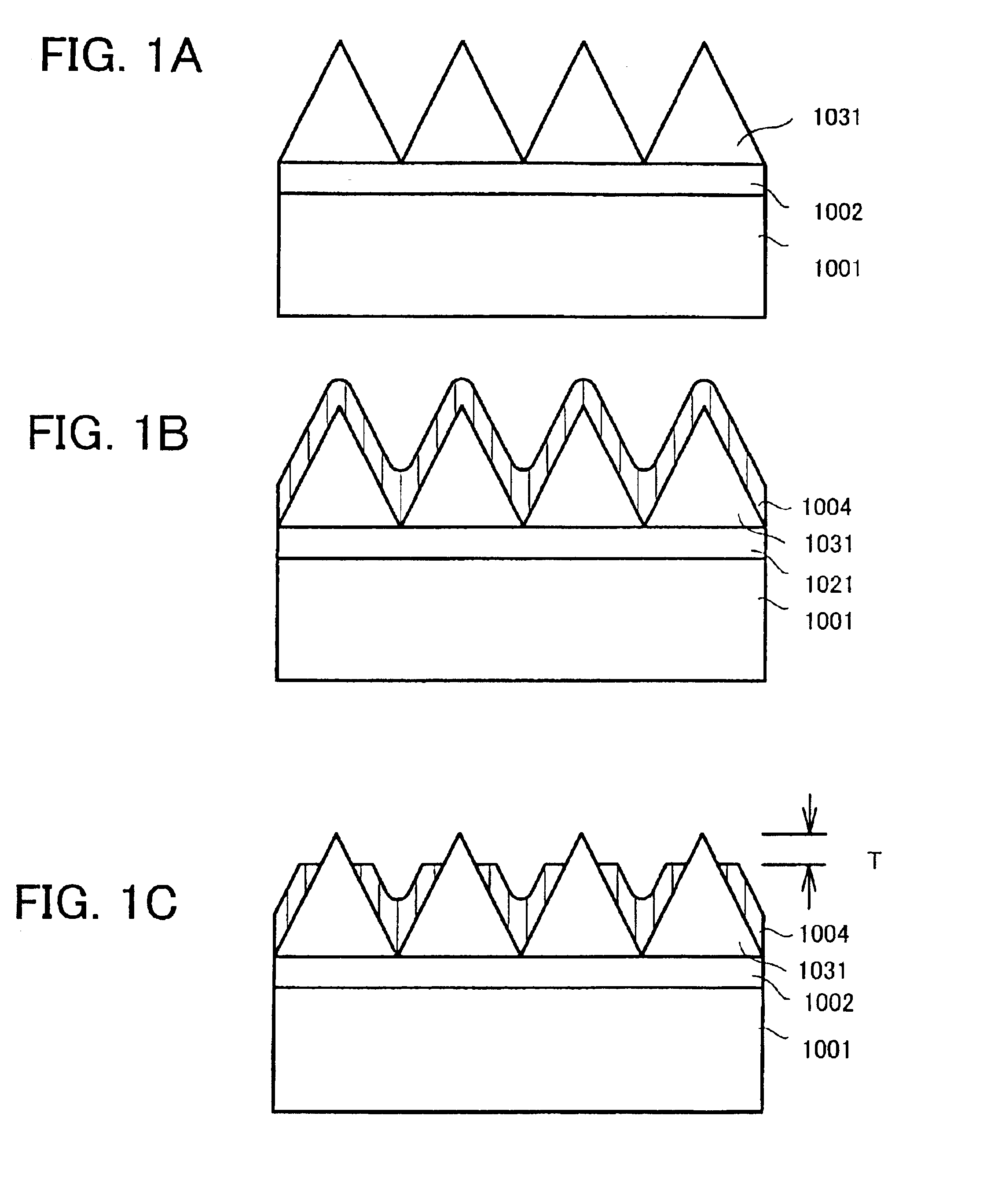
[0102][Second Embodiment]
[0103]In the present embodiment, as shown in FIGS. 4 and 5, an underlying layer including multiple layers was employed. A monocrystalline sapphire substrate 1001 having an a-plane as a primary crystal plane was cleaned through organic cleaning and heat treatment. The temperature of the substrate 1001 was lowered to 400° C., and H2 (10 L / min), NH3 (5 L / min), and TMA (20 μmol / min) were fed for about three minutes, to thereby form a first AlN layer (first buffer layer) 1021 (thickness: about 40 nm) on the substrate 1001. Subsequently, the temperature of the sapphire substrate 1001 was maintained at 1,000° C., and H2 (20 L / min), NH3 (10 L / min), and TMG (300 μmol / min) were introduced, to thereby form a GaN layer (intermediate layer) 1022 (thickness: about 0.3 μm). Subsequently, the temperature of the substrate 1001 was lowered to 400° C., and H2 (10 L / min), NH3 (5 L / min), and TMA (20 μmol / min) were fed for about three minutes, to thereby form a second AlN layer (...
third embodiment
[0106][Third Embodiment]
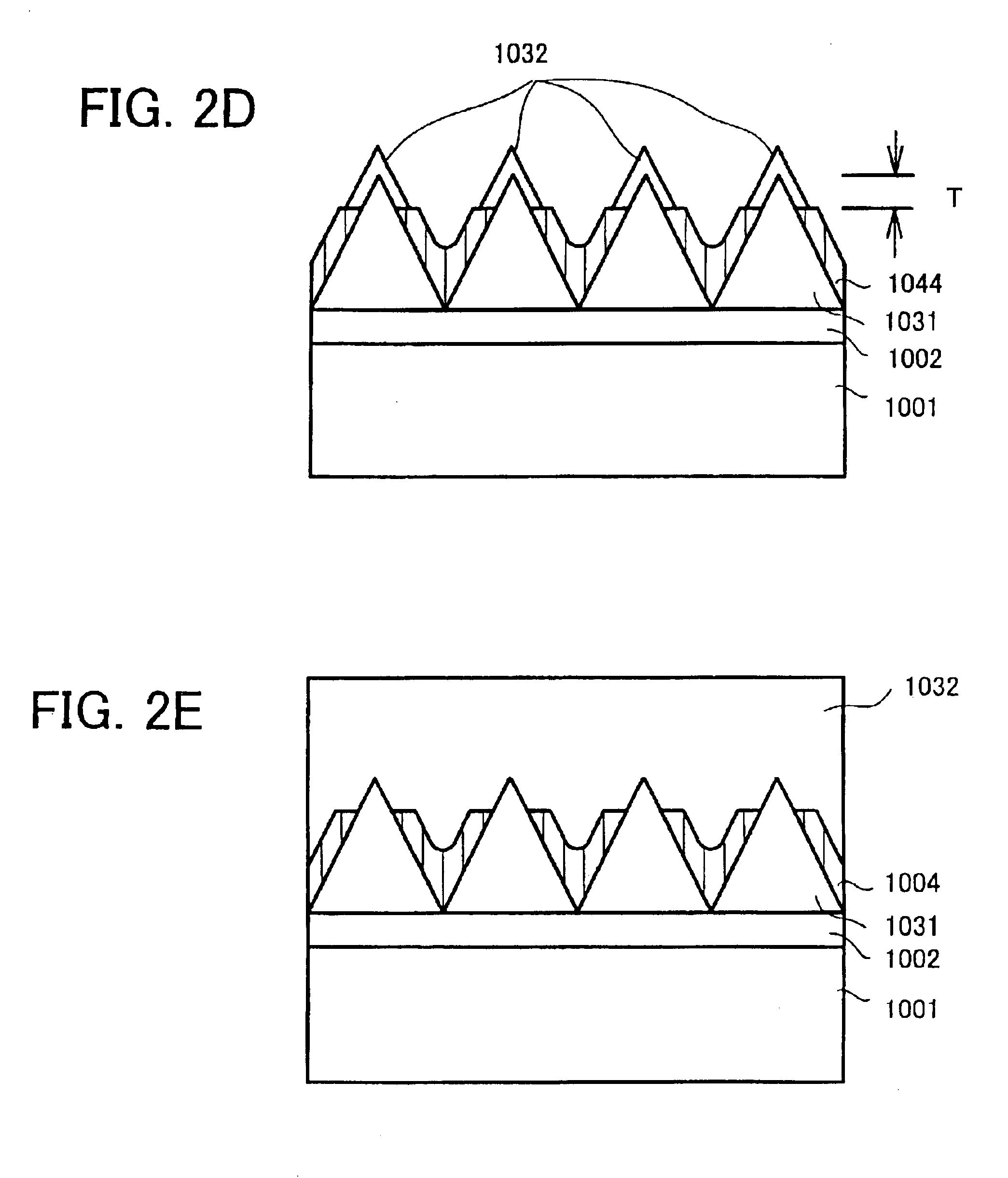
[0107]In the present embodiment, the first embodiment was modified such that, in formation of the GaN layer 1031, the GaN layer 1031 was doped with TMI to become a GaN:In layer 1031. The doping amount of indium (In) was regulated to about 1×10¹⁶ / cm3. Subsequently, in a manner substantially similar to that of the first embodiment, etching was performed; a tungsten mask 1004 was formed; the GaN:In layer 1031 was subjected to selective etching to thereby expose tops of the layer 1031; and lateral epitaxial growth of GaN was performed. The threading dislocations contained in a GaN layer 1032 which was laterally grown on the GaN:In layer 1031 serving as nuclei for crystal growth were slightly reduced in number as compared with those contained in the GaN layer 1032 formed in the first embodiment.
PUM
 Abstract
Description
Claims
Application Information