Dual-imaging optical system

Inactive Publication Date: 2005-03-15
NIKON CORP
View PDF44 Cites 0 Cited by
  • Summary
  • Abstract
  • Description
  • Claims
  • Application Information

AI Technical Summary

Benefits of technology

This invention provides a dual-imaging optical system that can effectively correct distortion to a high degree while providing a compact optical system, maintaining imaging performance, and correcting for manufacturing tolerances.
In order to correct distortion or astigmatism, correct accumulated manufacturing tolerances, and not create other types of distortion, a correcting optical system in the form of at least one aspheric optical surface is placed near the intermediate image. The placement of an aspheric correcting optical system near the intermediate image is especially effective for correcting higher-order distortion or astigmatism. A lens with an aspheric surface may be used for this purpose. On the other hand, since the reflecting surface is near the intermediate image, the reflecting surface itself may be made aspheric and used as the correcting optical system. The reflecting surface can be placed very close to or even at the intermediate image, so that making the reflecting-surface aspheric allows designation of the desired distortion or astigmatic-aberration correction in a straightforward manner, with little effect on other types of aberration.
From the point of view of machining the aspheric surface, simplicity is preferred, such that an axially symmetric surface or one which can change in a longitudinal direction only (a circular or non-circular cylindrical surface) would be better.
The above-summarized invention allows near-perfect correction of the particular aberrations which increase with reductions in the size of the optical system, and even near-perfect correction of hard-to-correct higher-order aberration and distortion and aberration due to manufacturing, while avoiding almost all effects on other aberrations, such as spherical aberration, coma aberration, sine conditions, and axial chromatic aberration.

Problems solved by technology

The Abbe numbers of fused silica and fluorite are not sufficiently different from each other to allow complete correction of chromatic aberration.
For this reason, at wavelengths of 300 nm or below, it is extremely difficult to correct chromatic aberration in projection-optical systems comprised solely of standard refractive optical systems.
The refractive index of fluorite changes relatively rapidly with variations in temperature, and fluorite polishes poorly.
Thus, many optical systems do not use fluorite, resulting in systems with lenses of fused silica only.
Such all-silica systems exhibit uncorrectable chromatic aberration.
Purely reflective optical systems avoid chromatic aberration, but such systems tend to be excessively large, and to require one or more aspheric reflecting surfaces.
The production of (large) precision aspheric surfaces is extremely difficult.
In optical systems utilizing several mirrors, it is possible to reduce the number of refractive lenses, but other problems arise.
But, in a catadioptric imaging system, as, for example, in U.S. Pat. No. 4,779,966, there is often no location for an effective aperture stop.
Even if it were possible to realize an optical system with a high NA, many optical elements would have to be placed along a limited optical-path length, so that the distance between the wafer and the nearest surface of the objective lens (i.e., the working distance WD) would be undesirably short.
The adjustment procedure for the eccentric sections of such optical systems is difficult and makes the realization of precision systems essentially impossible.
While this dual-imaging optical system has many superior features, attempts to reduce the size of the optical system while maintaining image-forming performance result in increased distortion.
That is, the optical system is not symmetric, so even if other aberrations are corrected, distortion will remain.
Also, when trying to correct distortion, astigmatism correction may be affected, and it is well known that it is extremely difficult to correct both types of aberration at the same time.
In the manufacturing of high-precision optical systems, variance from product to product inevitably arises due to manufacturing tolerances.
This variance results in different aberration levels for each optical system produced.
However, when there is asymmetric aberration of differing amounts across the image surface due to manufacturing tolerances, or when the generated aberration amounts are too great, it is often impossible to fully correct the system for manufacturing tolerances solely by adjusting sections of the optical system.
While such a correcting plate is effective in correcting “angle-of-view” aberrations (such as distortion and / or astigmatism) when placed as close as possible to the image surface, in practice, the presence of other adjusting devices or measuring equipment near the image surface normally requires that such plates be placed a sufficient distance away from the image surface such that other types of aberration (related to aperture) are also affected.
This complicates the correction process.

Method used


Image

  • Dual-imaging optical system
  • Dual-imaging optical system
  • Dual-imaging optical system

Examples


example embodiment 1

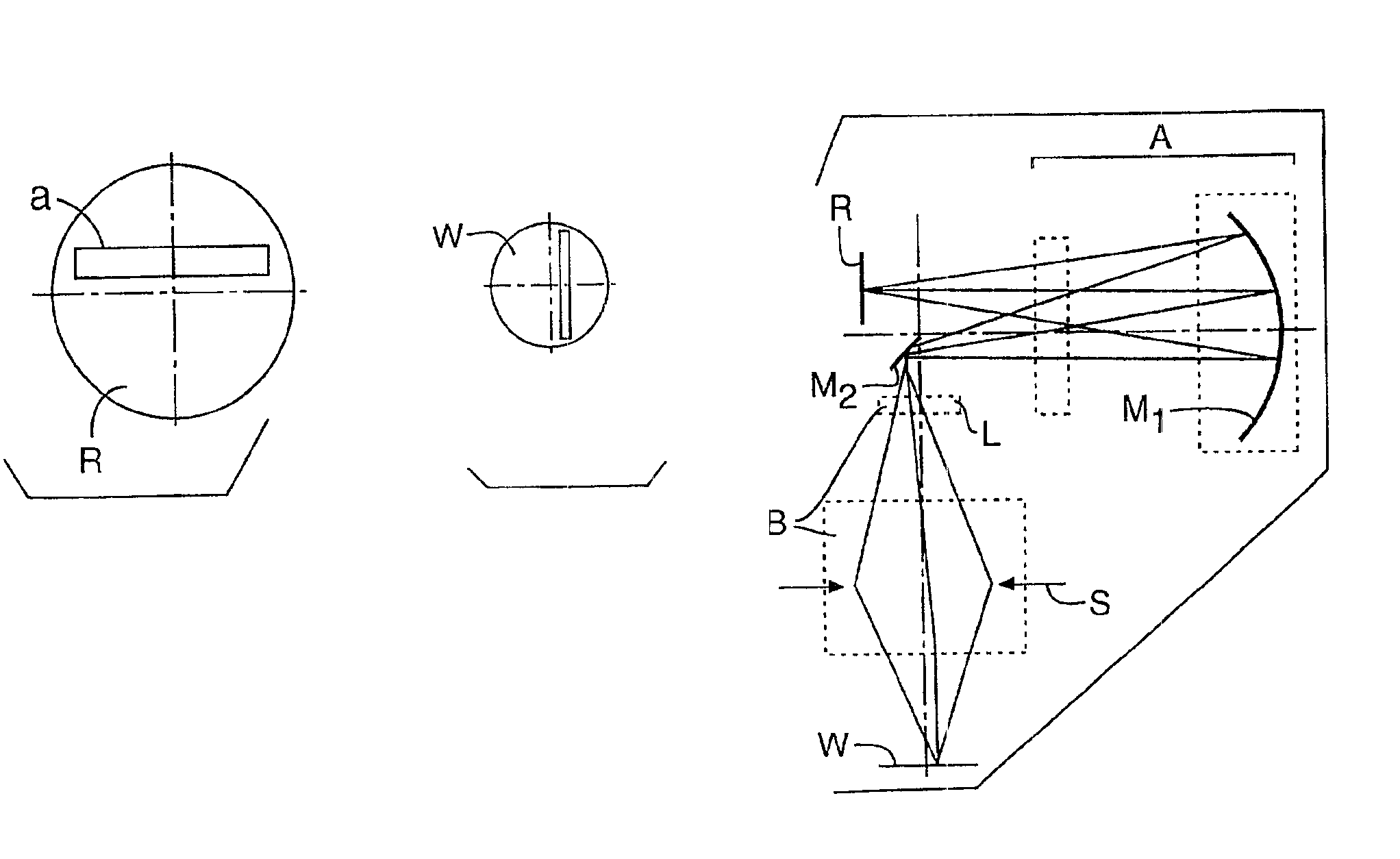
FIG. 3 shows an optical-path diagram of Example Embodiment 1 of a catadioptric optical system according to the present invention. As shown in FIG. 3, an excimer laser E is configured to illuminate the reticle R. The optical system of FIG. 3 can be used with the respective embodiment of FIGS. 1(a)-1(c) or of FIGS. 2(a)-2(c). In FIG. 3, the reflecting surface M2 is planar, and the surface of lens element L in the optical system nearest to the reflecting surface M2 is aspheric.

FIG. 4 shows an expanded optical-path diagram of Example Embodiment 1. That is, in order to avoid the complications of reflected light in the drawings, the light rays are shown in FIG. 4 as always propagating in the same direction.

Table 1 below lists the surface data of Example Embodiment 1. The optical path of FIG. 4 is set forth in Table 1 with the reflecting surface M3 omitted and with a flat reflecting surface inserted, as surface 10, to represent the unfolding of the optical path as shown in FIG. 4. In Table...

example embodiment 2

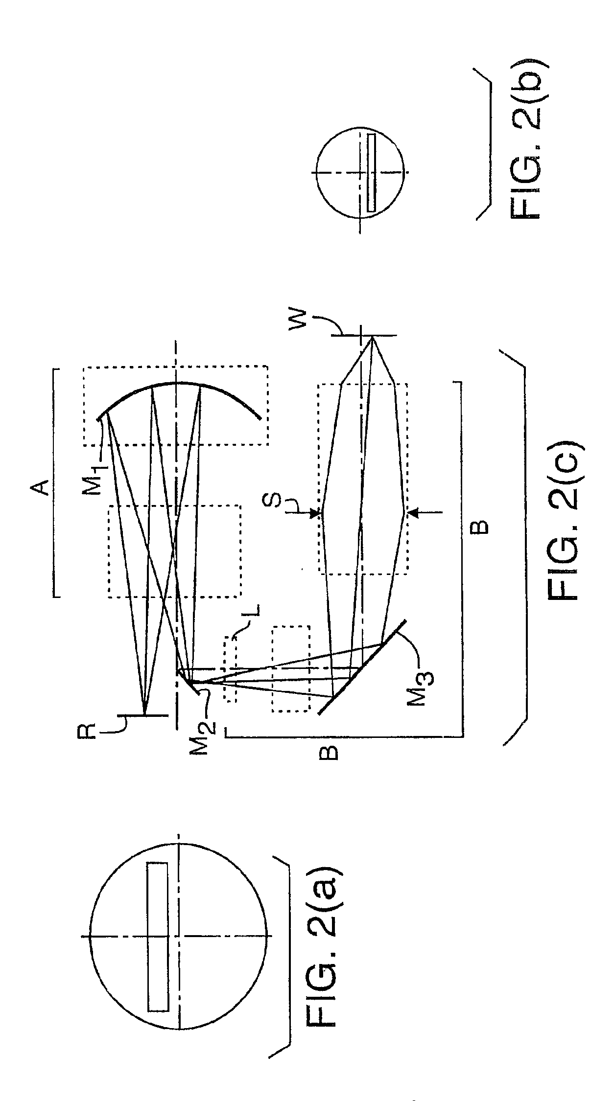
FIG. 6 shows an optical path diagram of Example Embodiment 2 of a catadioptric optical system according to the present invention. The optical system of FIG. 3 can be used with the respective embodiment of FIGS. 1(a)-1(c) or of FIGS. 2(a)-2(c). In FIG. 3, the reflecting surface M2 is aspheric, and the optical surface of lens L in the optical system B nearest to the reflecting surface M2 is spherical.

Table 3 below lists the surface data of Example Embodiment 2. An optical path corresponding to FIG. 1 is set forth in Table 3, with the mirror M3 omitted. As in Table 1, in Table 3, the first column lists the surface number from the reticle R; the second column, labeled “r”, lists the radius of curvature for each of the surface; the third column, labeled “d”, lists the axial distance from each surface to the next surface; the fourth column list the material for each lens; and the fifth column lists the group designation for each optical element. The surface featuring an asterisk (*) in th...


PUM


Abstract

An optical imaging system especially for microlithography includes a first imaging system forming an intermediate image of an object, and a second imaging system forming, on a surface, an image of the intermediate image. A reflective surface directs light from the first imaging system to the second imaging system. An aspherical corrective optical surface is located at or near the location of the intermediate image for correcting aberrations such as high-order distortion, aberrations due to accumulation of manufacturing tolerances, and spherical aberration. The first imaging system comprises a positive power refractive element and a concave mirror. The second imaging system comprises refractive elements and no concave mirror.

Description

FIELD OF THE INVENTIONThis invention pertains primarily to optical systems used in reduction-type projection-exposure apparatus such as projection steppers and scanners used in the manufacture of semiconductors. The invention is especially directed to such apparatus that employ catadioptric optical systems in their optical systems with resolution in the sub-micron levels of the ultraviolet wavelengths.BACKGROUND OF THE INVENTIONAs circuit patterns for semiconductors become finer, higher levels of resolution are demanded of steppers and scanners that expose these patterns. To satisfy demands for higher resolution, the wavelength of the radiation employed must be reduced, and the numerical aperture (NA) of the optical system must be increased.Only a few optical materials are adequately transmissive at shorter wavelengths. For wavelengths of 300 nm or less, the only currently available materials that can be used effectively are synthetic fused silica and fluorite.The Abbe numbers of fu...

Claims


Application Information

Patent Timeline
IPC IPC(8): G02B17/08G03F7/20
CPCG02B17/08G03F7/70275G03F7/70225G02B17/0892
Inventor TAKAHASHI, TOMOWAKI
Owner NIKON CORP
Why Eureka
Try Eureka