Anisotropic conductive sheet and wafer inspection device

Inactive Publication Date: 2005-03-22
ISC CO LTD
View PDF15 Cites 18 Cited by
  • Summary
  • Abstract
  • Description
  • Claims
  • Application Information

AI Technical Summary

Benefits of technology

The present invention has been made on the basis of the foregoing circumstances and has as its object the provision of a wafer inspection apparatus which is suitable for use in conducting electrical inspection of a great number of integrated circuits formed on a wafer, which can be miniaturized as a whole, is prevented from shortening the

Problems solved by technology

It takes a long time to conduct inspection of the circuit device composed of the semiconductor chip, and inspection cost becomes considerably high because the semiconductor chip is minute, and its handling is inconvenient.
(1) In the wafer inspection apparatus shown in FIGS. 13 and 15, it is necessary to press the connecting pins under pressing force of about 0.8 N (about 0.08 kgw) per pin for the purpose of achieving stable electrical connection of the input-output terminals 87 of the controller 85 to the respective leading terminals 82 of the circuit board 80 for inspection. Accordingly, when the number of, for example, leading terminals 82 of the circuit board 80 for inspection is, for example, 5,000, pressing force of about 4,000 N is required as a whole. Therefore, the apparatus involve a problem that a pressing mechanism for applying such pressing force inevitably becomes large in size, and a large-scaled member that withstands great pressing force is also required for the holding member for the circuit board 80 for inspection, so that the whole wafer inspection apparatus becomes considerably large in size.
The apparatus also involve a problem that the service life of the circui

Method used


Image

  • Anisotropic conductive sheet and wafer inspection device
  • Anisotropic conductive sheet and wafer inspection device
  • Anisotropic conductive sheet and wafer inspection device

Examples


Example

[Production Example 1 of Mold]

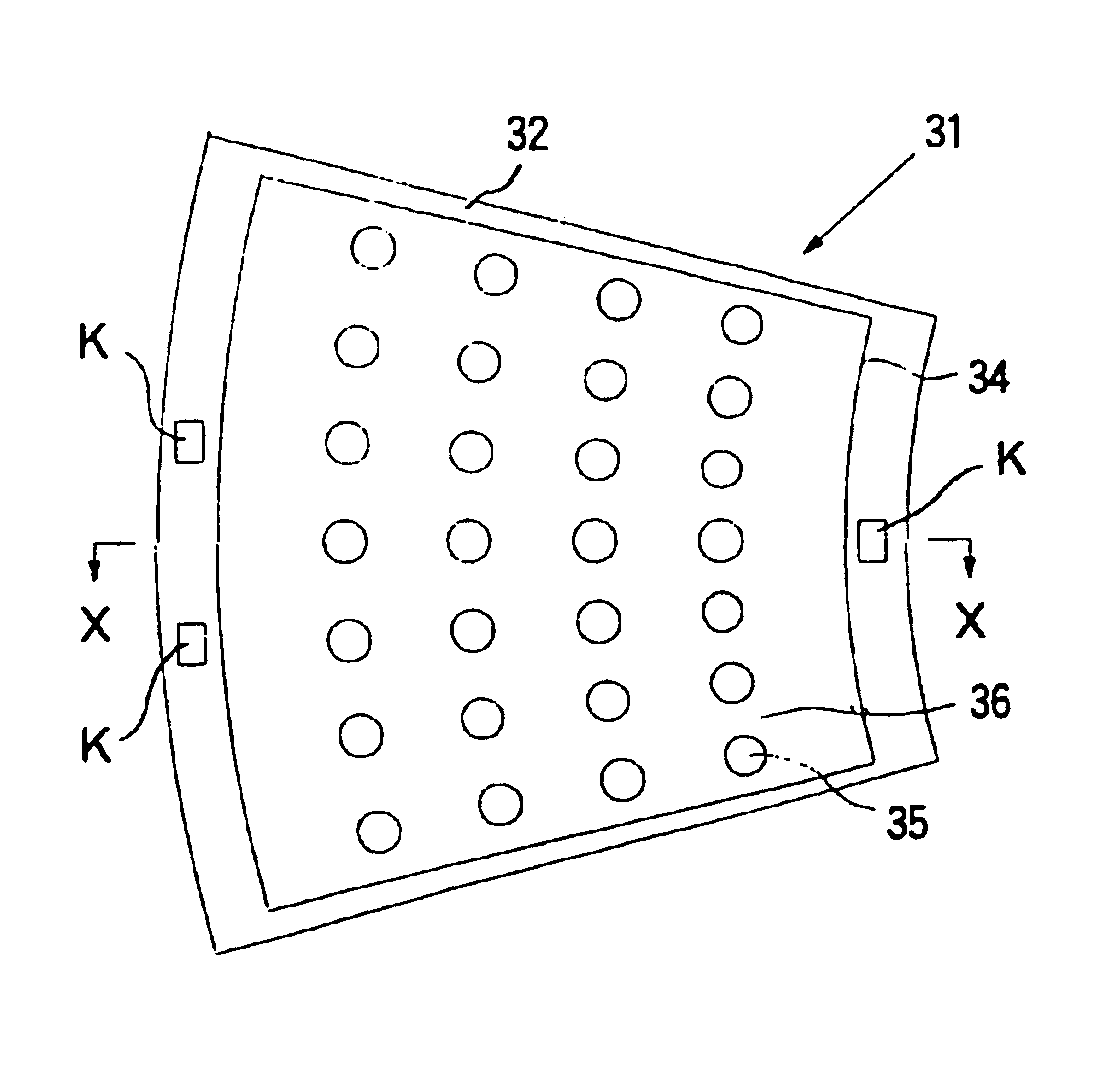
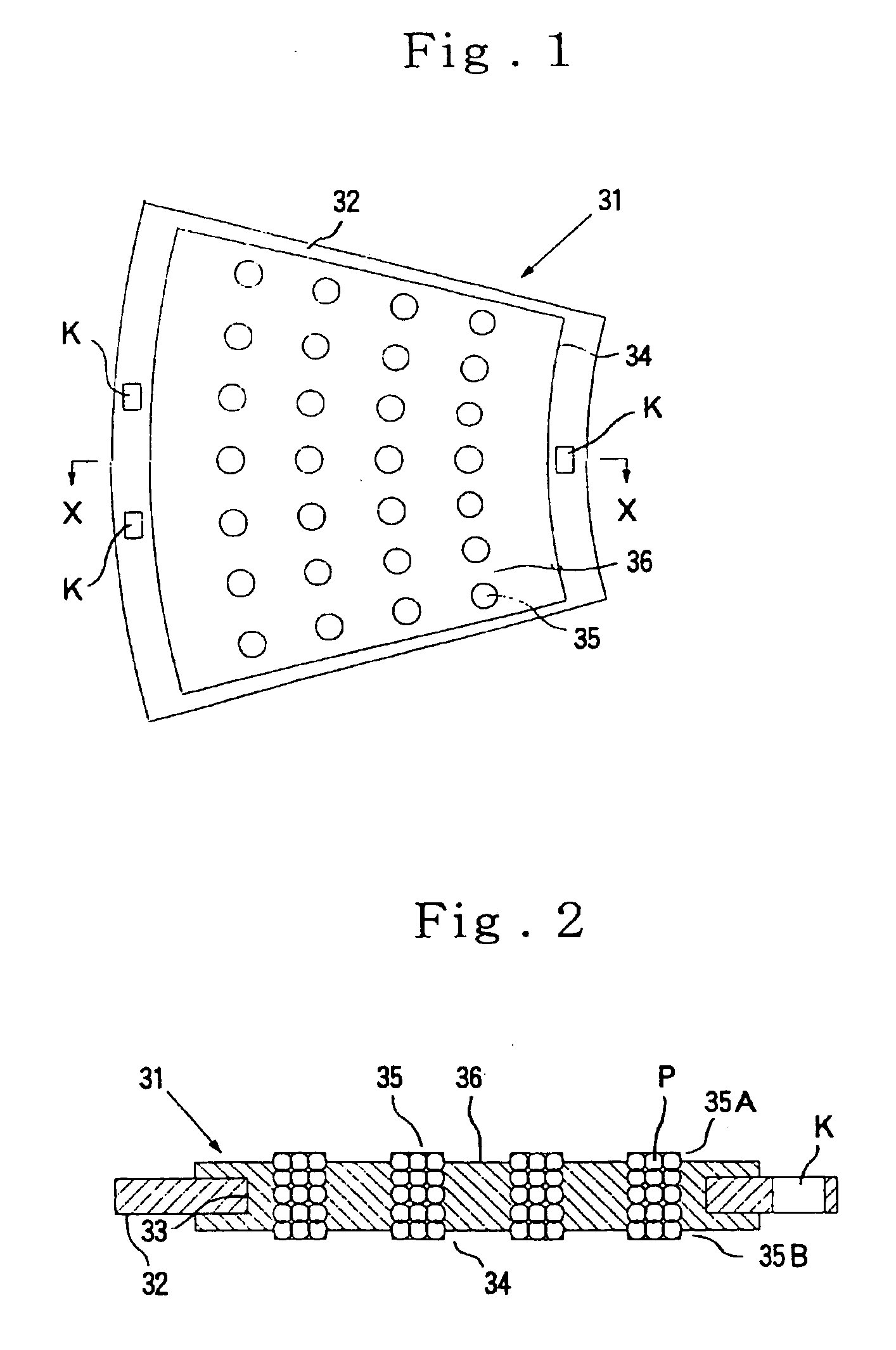
A brass plate having a thickness of 3.0 mm was provided, a plurality of recesses for receiving a magnetic member, which each had a circular section whose diameter was 1.0 mm and depth was 2.7 mm, were formed in one surface of such a non-magnetic base plate by a drilling machine at a pitch of 2 mm in an X—X direction (the direction meaning a direction corresponding to the X—X direction in FIG. 1 or FIG. 6; the same shall apply hereinafter), and a plurality of recesses for forming a projected portion, which each had a circular section whose diameter was 0.8 mm and depth was 0.2 mm, were formed in the other surface of the non-magnetic base plate at a pitch of 2 mm in the X—X direction, thereby producing a non-magnetic base plate. A spherical magnetic member made of iron having a diameter of 1.0 mm was arranged in each of the recesses for receiving the magnetic member in this non-magnetic base plate, and a columnar lid member having a thickness of 1.7 mm an...

Example

[Production Example 2 of Mold]

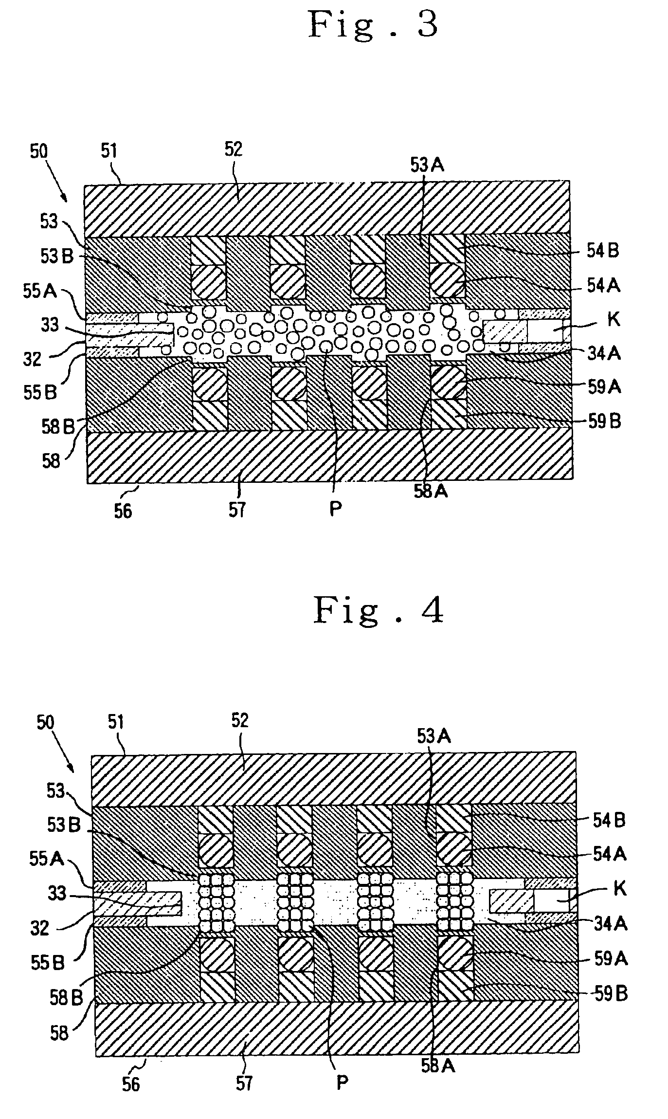
An iron plate having a thickness of 6 mm was provided, and one surface of this iron plate was subjected to a photoetching treatment using a dry film resist and ferric chloride, thereby producing an intermediate in which a plurality of disk-like ferromagnetic substance layers each having a thickness of 0.1 mm and a diameter of 0.5 mm had been integrally formed at a pitch of 1.27 mm in the X—X direction in a ferromagnetic base plate made of iron having a thickness of 5.9 mm.

Non-magnetic substance layer having a thickness of 0.2 mm was formed at other area than the ferromagnetic substance layers in said one surface of the intermediate by using a resist, thereby making a top force. A bottom force was made in the same manner as in the production of the top force to produce a mold of the construction shown in FIG. 5. This mold is referred to as “Mold b”.

Example

EXAMPLE 1

An insulating sheet body composed of a glass fiber-reinforced epoxy resin (modulus of elasticity: 2×10⁹ Pa; coefficient of linear thermal expansion: 1.5×10⁻⁵ K−1; saturation magnetization: 0 wb / m2) and having a thickness of 0.4 mm, in which a great number of through-holes each having a circular section of 1.8 mm in a diameter had been formed at a pitch of 2.0 mm in the X—X direction, was produced, and 2 spacers composed of stainless steel (SUS-304) having a thickness of 0.6 mm, in which a great number of through-holes each having a circular section of 1.95 mm in a diameter had been formed at a pitch of 2.0 mm in the X—X direction, were produced.

On the other hand, 6 g of conductive particles having a number average particle diameter of 120 μm were added to and mixed with 16 g of addition type liquid silicone rubber, “KE-2000-30” (product of Shin-Etsu Chemical Co., Ltd.), thereby preparing a molding material for molding an elastic anisotropically conductive film. As the condu...


PUM


Abstract

Disclosed herein are a wafer inspection apparatus which is small in size, prevented from shortening the service life of its circuit board for inspection, can collectively perform inspection as to a great number of electrodes to be inspected, has good electrical properties and can perform electrical inspection of high functional integrated circuits, and an anisotropically conductive sheet suitable for use in this wafer inspection apparatus. The anisotropically conductive sheet is composed of an insulating sheet body, in which a through-hole has been formed, and an elastic anisotropically conductive film arranged in the through-hole. The insulating sheet body is formed of a material having a modulus of elasticity of 1×10⁸ to 1×10¹⁰ Pa, a coefficient of linear thermal expansion of 3×10⁻⁶ to 3×10⁻⁵ K−1 and a saturation magnetization lower than 0.1 wb/m2, the elastic anisotropically conductive film is composed of a plurality of conductive path-forming portions and insulating portions formed among these conductive path-forming portions, the conductive path-forming portions are obtained by filling conductive particles having a number average particle diameter of 30 to 150 μm, a coating layer composed of a noble metal and having a thickness of at least 20 nm is formed on surfaces of the conductive particles, each of the conductive path-forming portions has a durometer hardness of 15 to 45, and an electric resistance between conductive path-forming portions is at least 10 MΩ.

Description

TECHNICAL FIELDThe present invention relates to a wafer inspection apparatus and an anisotropically conductive sheet suitable for use in the wafer inspection apparatus, and particularly to a wafer inspection apparatus for collectively conducting a probe test as to a part or the whole of a great number of integrated circuits formed on a wafer or a wafer inspection apparatus for collectively conducting a burn-in test as to the whole of a great number of integrated circuits formed on a wafer, and an anisotropically conductive sheet suitable for use in these wafer inspection apparatus.BACKGROUND ARTIn the production process of semiconductor integrated circuit devices, after a great number of integrated circuits are formed on a wafer, a probe test is generally conducted as to each of these integrated circuits. This wafer is then cut, thereby forming semiconductor chips. Such semiconductor chips are contained and sealed in respective proper packages. Each of the packaged semiconductor int...

Claims


Application Information

Patent Timeline
IPC IPC(8): G01R1/073G01R1/067
CPCG01R1/06755G01R1/07314G01R1/0735Y10T428/26Y10T428/256H01L22/00
Inventor INOUE, KAZUOIGARASHI, HISAO
Owner ISC CO LTD
Why Eureka
Try Eureka