ESD protection for semiconductor products

a technology of esd protection and semiconductor products, applied in the direction of semiconductor devices, semiconductor/solid-state device details, electrical apparatus, etc., can solve the problems of unintended conduction, thermal damage, and the effort to economically integrate esd protection devices on an integrated circuit requires compromises in performance or manufacturing costs, so as to reduce the current density and reduce the lateral current

Inactive Publication Date: 2005-03-29
SEMICON COMPONENTS IND LLC
View PDF5 Cites 54 Cited by
  • Summary
  • Abstract
  • Description
  • Claims
  • Application Information

AI Technical Summary

Benefits of technology

In accordance with this invention, an ESD device is provided with a P body implant that is wider than the contact via. As such, the invention performs the P body implant earlier in the fabrication process. In the preferred embodiment, the P body implant for the ESD device may be formed at the same time and the P body implant for a DMOS device. The P body implant for the ESD device is formed through an opening a resist mask. The same mask may be used for the P body of a DMOS device. Those skilled in the art understand that the opening for the P body implant can be made to any suitable size to accommodate the desired breakdown voltage of the ESD device. The larger P body implant, compared to the prior art ESD devices, reduces the lateral current and provides a lower current density during breakdown so that the maximum temperature increase due to breakdown occurs in the body of the device and not at a contact where contact metal may spike into the surface. By directing the breakdown current away from the lateral direction, the maximum current density occurs deeper in the body of the device, and not proximate the surface. The invention provides, in effect, a lateral NPN parasitic transistor with a larger emitter area than the emitter areas in conventional parasitic NPN devices. The larger emitter area is disposed beneath the surface of the substrate so that a significant amount of the breakdown current is directed initially vertically away from the surface toward the heterodoped region.

Problems solved by technology

In the past, parasitic devices associated with functional circuitry have sometimes provided unintended conduction paths that carry the ESD surge and create thermal damage along that path.
Generally, efforts to economically incorporate ESD protection devices on an integrated circuit require compromises either in performance or manufacturing costs.
As trends continue for increased circuit density and lower operating voltages it is becoming more of a challenge to avoid compromises between performance of functional circuitry and ESD circuitry.
More specifically, these trends make it increasingly difficult to effectively shunt heat away from thermally sensitive regions.
While it is desirable to optimize the ESD device turn-on voltage in order to provide maximum protection before damaging the functional circuitry, it is recognized that when the parasitic devices are optimized to provide ESD protection, there can be less satisfactory performance of the functional circuitry.
However, I found that the narrow p-implant tends to shift the ESD current laterally so that the ESD device directs the current beneath the gate and has too high a current density.
That defect is caused in part by the making the p-implant late the process where the contact opening is used as a mask for the P-type ions.
Another trend which limits the performance of ESD protection circuitry relates to marked decreases in gate breakdown voltages.

Method used


Image

  • ESD protection for semiconductor products
  • ESD protection for semiconductor products
  • ESD protection for semiconductor products

Examples


Embodiment Construction

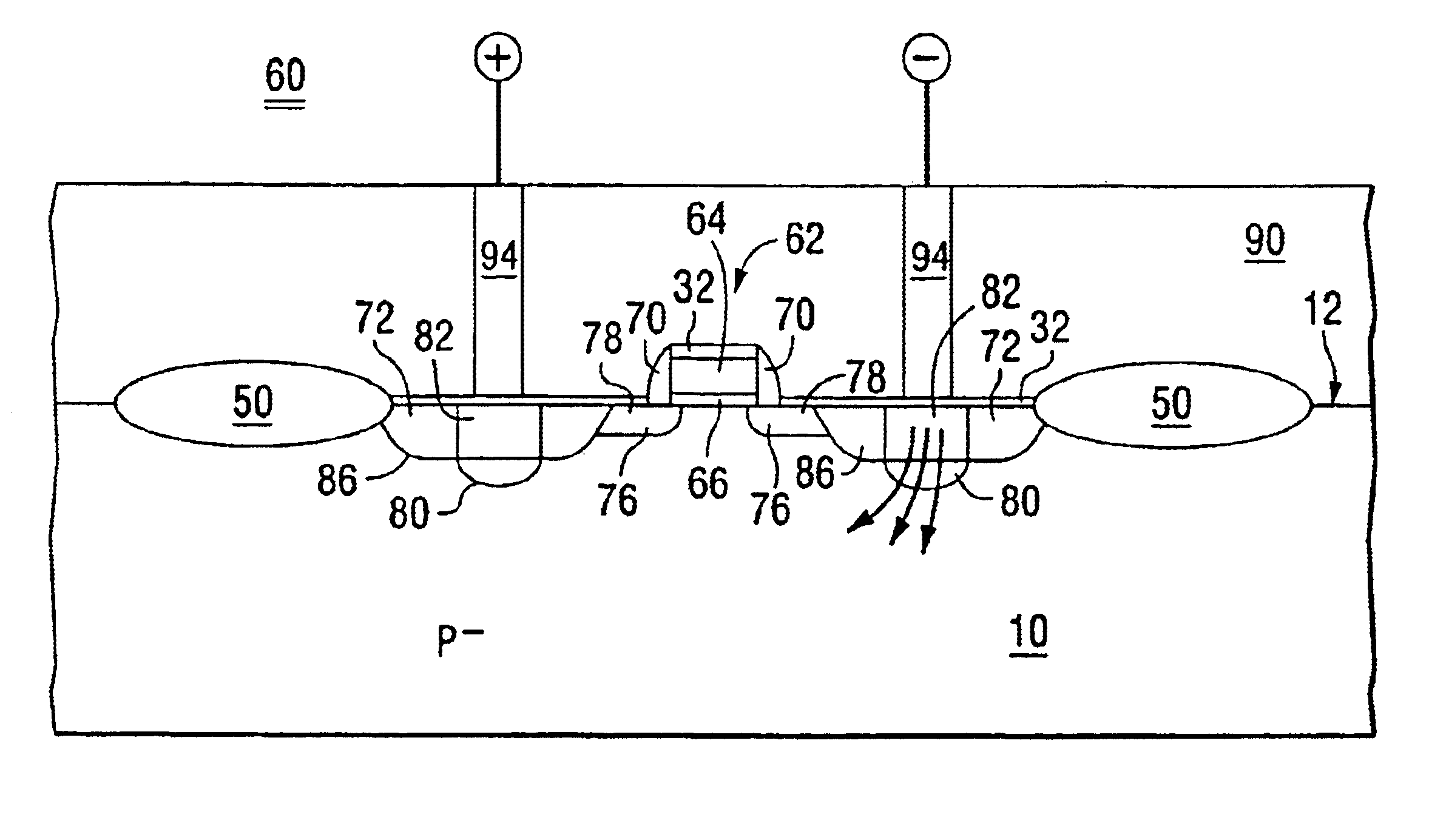
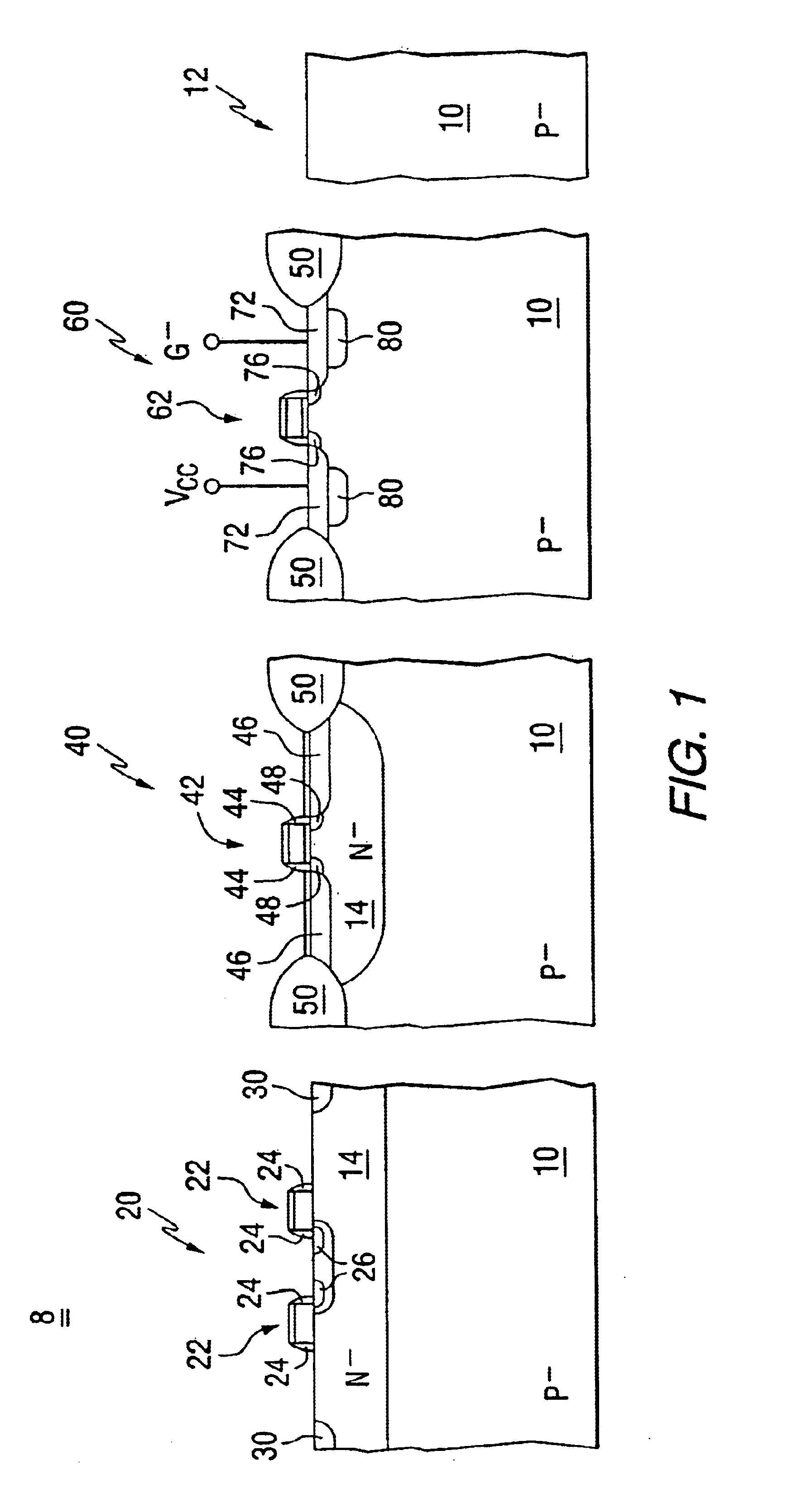
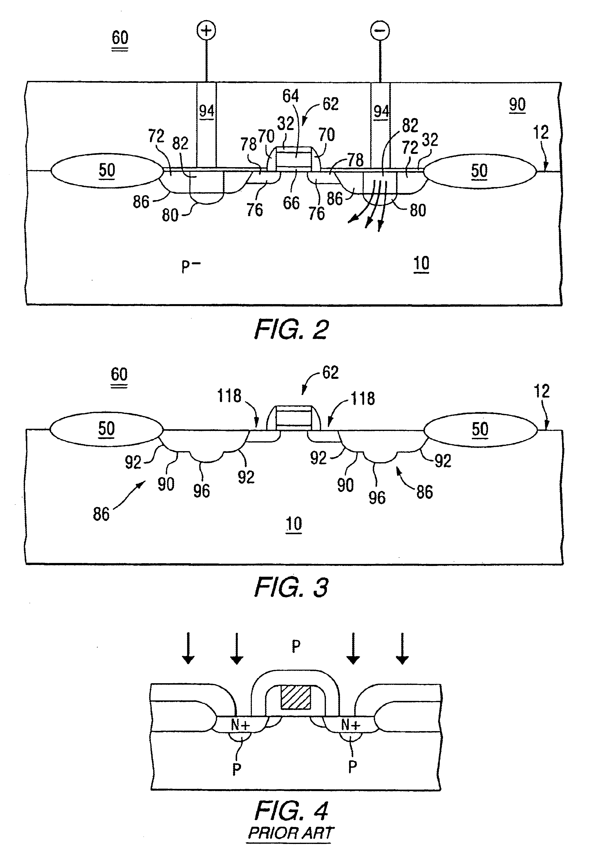
In the following descriptions any dimensions provided are with reference to distances taken along the corresponding view. In a cross sectional view, a width or lateral dimension is intended to mean a distance along a horizontal plane parallel with a plane semiconductor surface, while a height or depth is intended to mean a distance taken along a vertical dimension of the view, more or less orthogonal with the plane semiconductor surface. For purposes of comparing example embodiments of the invention with prior-known designs, it may be assumed that all devices illustrated are fabricated with the same photolithographic capability. The disclosed embodiments assume a minimum feature size, i.e., line width geometry, of 0.35 micron although the invention is applicable to a wide range of line width geometries, device densities and types of semiconductor products.

As used herein the term substrate means a layer over which or in which a structure such as a portion of a transistor device is fo...


PUM


Abstract

Device 60 in FIG. 3 has junctions 86 each with a lateral portion 90 and a second portion 92 extending upward toward the surface 12 from the lateral portion 90. The lateral portions 90, as illustrated in FIG. 3, are more or less formed along a plane parallel with the surface 12. The upwardly extending portions 92 include characteristic curved edges of the diffusion fronts which are associated with the planar process. With the regions 80 and 82 each having relatively high net dopant concentrations of different conductivity types, each lateral junction portion 90 includes a relatively large sub region 96 which extends more deeply into the layer 10. When compared to other portions of the junctions 86, the subregions 96 are characterized by a relatively low breakdown voltage so that ESD current is initially directed vertically rather than laterally.

Description

FIELD OF THE INVENTIONThis invention relates to semiconductor devices and, more particularly, to the provision of electrostatic discharge (ESD) protection of integrated circuitry.BACKGROUNDThe Field Effect Transistor (FET) has become the most common device used in integrated circuitry, providing a wide variety of electronic tasks, e.g., analog signal processing, memory functions, high speed, low power logic operations and power switching.During the last decade the semiconductor industry has more fully embraced the use of protection circuitry to shield FET's and other circuitry from damage associated with brief, high power voltage spikes such as the ESD. Because the FET is in many instances the prevalent device type on such circuitry it is often most convenient to form transistor protection devices coincident with the fabrication of FETs. This allows economy, i.e., avoidance of extra fabrication steps.Although formation of the protection device follows the process fabrication sequenc...

Claims


Application Information

Patent Timeline
Patent Type & Authority Patents(United States)
IPC IPC(8): H01L29/76H01L23/62H01L21/02H01L23/58H01L21/338H01L29/66H01LH01L27/02H01L29/78
CPCH01L29/7833H01L27/0266
Inventor CAI, JUNSUGERMAN, ALVINPARK, STEVEN
Owner SEMICON COMPONENTS IND LLC
Why Eureka
Try Eureka