Compound semiconductor multilayer structure and bipolar transistor using the same

Inactive Publication Date: 2005-04-05
SHOWA DENKO KK
3 Cites 7 Cited by

AI-Extracted Technical Summary

Problems solved by technology

However, conventional HBTs employing a carbon-doped GaAs-system crystal layer having a high carrier (hole) concentration of carbon (C) have been known to have a problem in that elemen...

Abstract

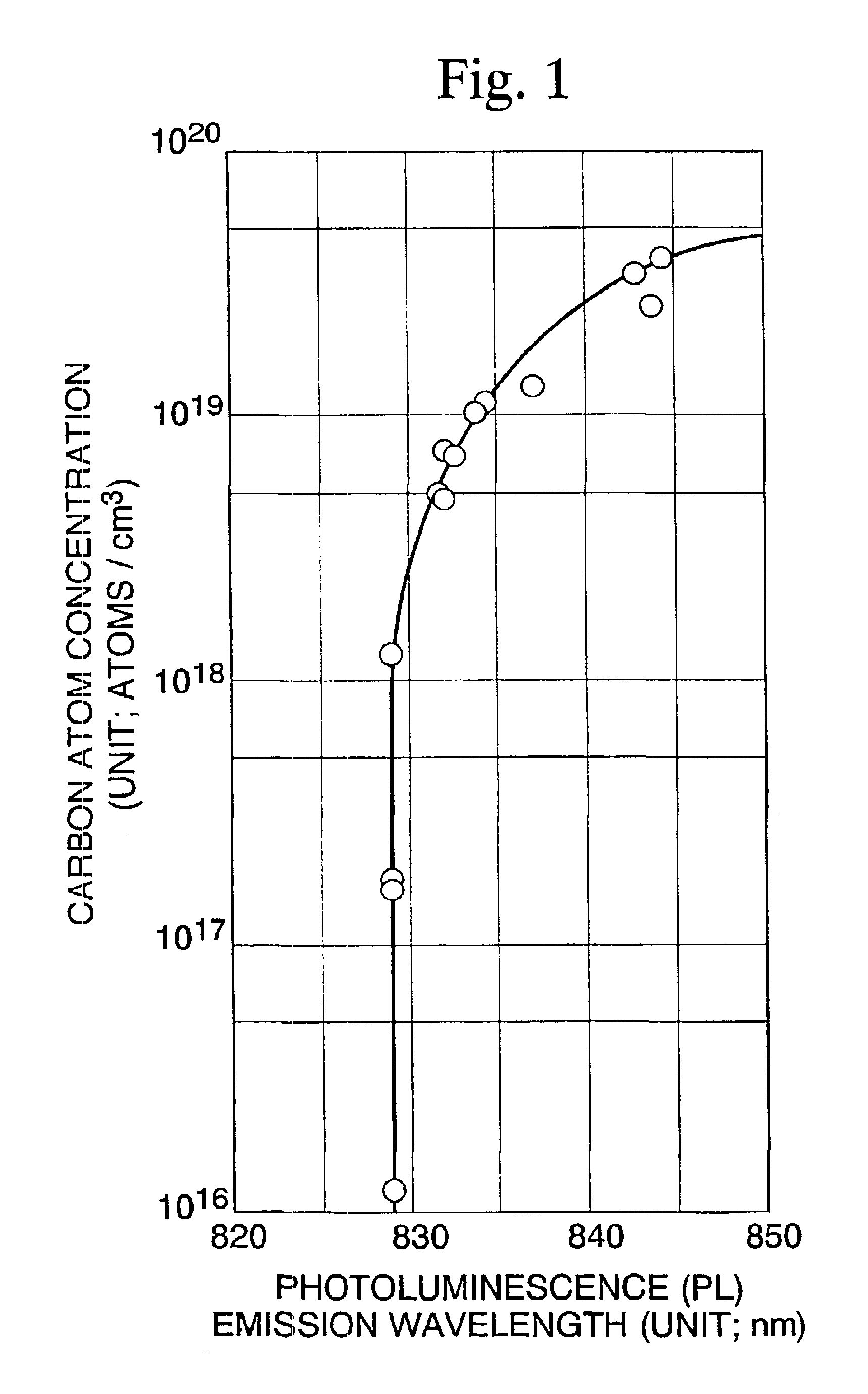
A compound semiconductor multilayer structure comprising a carbon-containing p-type gallium arsenide (GaAs)-system crystal layer, wherein the carbon-containing p-type GaAs-system crystal layer exhibits a predominant photoluminescence peak measured at 20K within a range of 828 nm to 845 nm, and wherein the ratio of hydrogen atom concentration to carbon atom concentration in the carbon-containing p-type GaAs crystal layer is 1/5 or less. Furthermore, in a photoluminescence measurement at 10K, the carbon-containing GaAs-system p-type crystal layer exhibits a first predominant photoluminescence peak and a second predominant photoluminescence peak due to band gap transitions of GaAs and wherein the second predominant luminescence wavelength has a longer wavelength than the first predominant photoluminescence wavelength and the intensity ratio of the second luminescence peak to the first luminescence peak is within a range from 0.5 to 3.

Application Domain

Polycrystalline material growthFrom chemically reactive gases +2

Technology Topic

Long wavelengthBand gap +10

Image

  • Compound semiconductor multilayer structure and bipolar transistor using the same
  • Compound semiconductor multilayer structure and bipolar transistor using the same
  • Compound semiconductor multilayer structure and bipolar transistor using the same

Examples

  • Experimental program(4)

Example

Example 1
[0065]The present invention will next be described in detail with reference to the case in which a GaxIn1-xP-system HBT is fabricated. FIG. 4 is a schematic cross-sectional view of an HBT 100 according to the present invention.
[0066]In an epitaxial multilayer structure for producing the HBT 100, a substrate 101 was formed of an undoped semi-insulating (100) 2° off GaAs single crystal. The GaAs single crystal serving as the substrate had a specific resistance at room temperature of approximately 2×10⁸ Φ·cm. On the upper surface of the substrate 101, which had a diameter of approximately 100 mm, was deposited a superlattice structure of an AlcGa1-cAs/GaAs system serving as a buffer layer 102. The superlattice structure was formed of an undoped Al0.3Ga0.7As layer 102a having an aluminum compositional proportion (=c) of 0.30, and an undoped p-type GaAs layer 102b. The undoped Al0.3Ga0.7As layer 102a had a carrier concentration of less than 5×1013 cm−3 and a thickness of 45 nm, while the p-type GaAs layer 102b has a carrier concentration of less than 1×1014 cm−3 and a thickness of 50 nm. Five of each of Al0.3Ga0.7As layer 102a with the above thickness and the p-type GaAs layer 102b with the above thickness were formed alternatingly in the number of five each. Each of the Al0.3Ga0.7As layer 102a and the p-type GaAs layer 102b was formed at 640° C. through reduced pressure MOCVD employing the (CH3)3Ga/(CH3)3Al/AsH3/H2 reaction system. The pressure during film formation was approximately 1.3×10⁴ Pa, and hydrogen was employed as a carrier gas.
[0067]On the buffer layer 102, an n-type Si-doped GaAs layer was formed as a sub-collector layer 103-1, through reduced-pressure MOCVD employing a (CH3)3Ga/AsH3/H2 reaction system. The GaAs layer serving as the sub-collector 103-1 has a carrier concentrations of 4×1018 cm−3, and the carrier concentration was adjusted by controlling the amount of disilane (Si2H6) supplied to the MOCVD reaction system. The layer had a thickness of 500 nm. On the sub-collector layer 103-1, an Si-doped GaAs layer was formed as a collector layer 103-2. The collector layer had a carrier concentration of 1×1016 cm−3, and a thickness of 600 nm.
[0068]On the n-type GaAs collector layer 103-2, a carbon-doped p-type GaAs layer was formed as a p-type base layer 104 by controlling the ratio of AsH3 to (CH3)3Ga (i.e., V/III ratio) supplied to the reaction system to 1.2. The base layer 104 had a carrier concentration of 3×1019 cm−3 and a thickness of 45 nm.
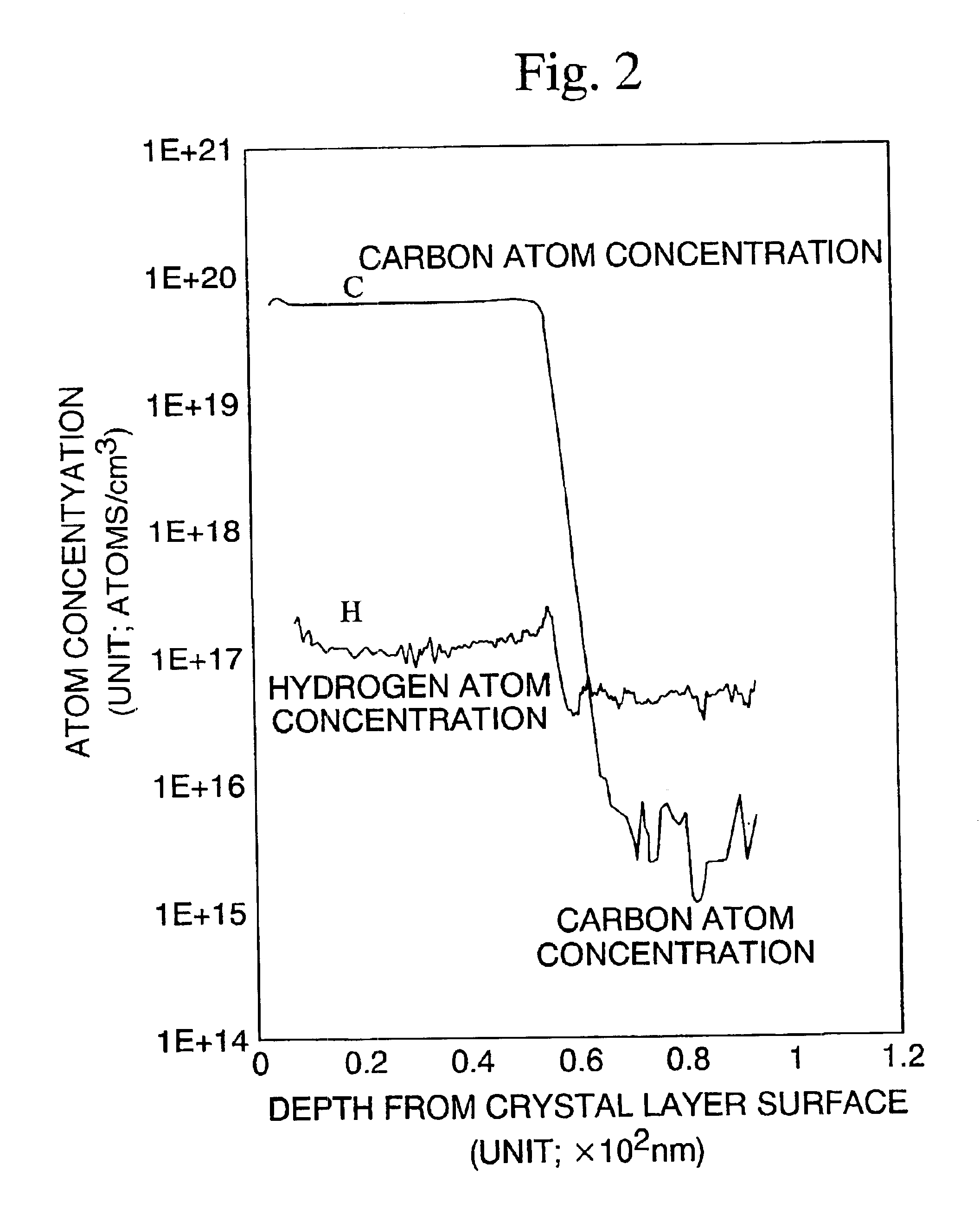
[0069]After completion of the growth to form the p-type base layer 104, the growth system was maintained at 640° C. without carrying out the subsequent growth prior to forming the emitter layer 105. During the intermission, the flow of hydrogen (H2) gas, which serves as a carrier gas in the MOCVD reaction system during vapor growth, was maintained. After completion of intermission for precisely five minutes, an n-type Ga0.49In0.51P emitter layer 105 (carrier concentration=4×1017 cm−3 and a thickness of 30 nm) was formed in a reduced pressure MOCVD system employing the (CH3)3Ga/(CH3)3Al/AsH3/H2 reaction system. In addition, a Si-doped n-type Ga0.5 In0.5As layer serving as an ohmic contact layer 106 (carrier concentration=6×1018 cm−3 and a thickness of 60 nm) was deposited on the emitter layer 105, to thereby complete formation of a multilayer structure 1A for producing npn-type HBTs. After completion of vapor growth to form the multilayer structure 1A, the reaction system was filled with nitrogen N2), and the temperature was lowered from 640° C. to 350° C. at 30° C./minute and from 350° C. to room temperature without special cooling. Through the cooling steps, the hydrogen atom (proton) concentration in the carbon-doped GaAs base layer was reduced to 2.0×10¹⁸ atoms/cm3.
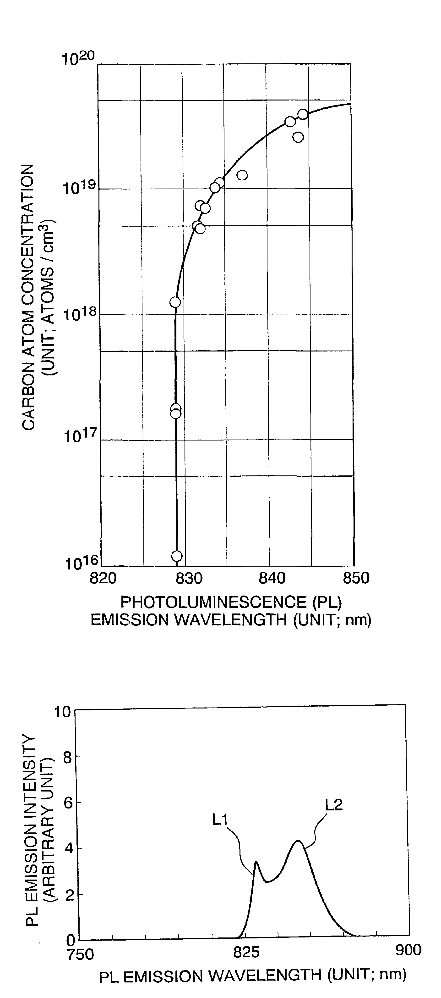
[0070]FIG. 6 shows a PL spectrum of a carbon-doped p-type GaAs layer at 20K. The predominant emission wavelength of PL was 844 nm. Conventional SIMS analysis revealed that the carbon atom concentration in the carbon-doped GaAs base layer 104 was determined to be 4.3×10¹⁹ atoms/cm3.
[0071]FIG. 3 shows a PL spectrum of a carbon-doped p-type GaAs layer at 10K. Two predominant emission wavelengths of PL were observed and the first predominant emission wavelength was observed at 830 nm and the second predominant wavelength was observed at 852 nm. The ratio of the intensity of the first predominant wavelength to that of the second predominant wavelength was 1.3. Conventional SIMS analysis revealed that the carbon atom concentration in the carbon-doped p-type GaAs layer 104 was determined to be 4.3×10¹⁹ atoms/cm3.
[0072]As shown in FIG. 4, a cross-sectional structure, in which a surface of the p-type base layer 104 and the surface of the n-type collector layer 103-2 are exposed, was formed by wet-etching of the aforementioned multilayer structure. On each exposed surface portion of the base layer 104, a p-type ohmic base electrode 107 made of a gold-zinc alloy was formed. On the exposed surface portion of the collector layer 103, an n-type ohmic collector electrode 108 made of a gold-germanium alloy was formed. On the surface of the remained emitter layer 105, an n-type ohmic emitter electrode made of a gold-germanium alloy was formed. Thus, the npn-type GaInP HBT 100 was fabricated.
[0073]The thus-fabricated HBT 100 exhibits a current gain (Ic/Ib:β) of 110 and a β drift as low as 0.5%.

Example

Comparative Example 1
[0074]The procedure of Example 1 for producing an npn-type GaInP-system HBT having a structure as shown in FIG. 3 was repeated, except that the following portions were changed, to thereby produce a similar element.
[0075]On the GaAs collector layer 103-2 as described in Example 1, a carbon-doped p-type GaAs layer was formed as a p-type base layer 104, by controlling the ratio of AsH3 to (CH3)3Ga (i.e., V/III ratio) supplied to the reaction system to 0.9. The carbon-doped p-type GaAs layer serving as the base layer 104 has a carrier concentration of 4×1019 cm−3 and a thickness of 45 nm, which were similar to those of Example 1. FIG. 7 shows a similar PL spectrum at 20K. The predominant emission wavelength of PL was 852 nm, which was 8 nm longer than the wavelength observed in Example 1. The reason for the red shift of the PL emission wavelength as compared with Example 1 is that the carbon atom concentration was as high as 6.9×10¹⁹ atoms/cm3. Furthermore, a carrier concentration of approximately the same level was disadvantageous, since the GaAs layer had a hydrogen atom concentration as well as a high carbon atom concentration.
[0076]After completion of the growth to form the p-type base layer 104, the growth system was maintained at 640° C. without carrying out the subsequent growth prior to forming the emitter layer 105 identical with that of Example 1. During the intermission, the flow of hydrogen (H2), which serves as a carrier gas in the MOCVD reaction system during vapor growth, was maintained. After completion of intermission for precisely five minutes, the emitter layer 105 and the ohmic contact layer 106 are stacked, to thereby complete formation of a multilayer structure for producing npn-type HBTs. After completion of the growth for producing the multilayer structure, the system was allowed to stand in a hydrogen atmosphere so as to lower the temperature from 640° C. to room temperature. Through the cooling steps, the hydrogen atom concentration in the carbon-doped GaAs base layer 104 was reduced to 2.2×10¹⁹ atoms/cm3. The difference between the carbon atom concentration and the hydrogen atom concentration in the carbon-doped GaAs base layer 104 was approximately equal to the carrier concentration (=4×10¹⁹ atoms/cm3) in the same layer 104.
[0077]In a manner similar to that of Example 1, an npn-type GaInP HBT 100 was fabricated from the formed multilayer structure. The HBT 100 exhibited a current gain (Ic/Ib:β) of 50 and a β drift as high as 1.5%.

Example

Comparative Example 2
[0078]An npn-type GaInP-system HBT having the same structure as that of Example 1 was formed except that the carbon-containing p-type GaAs layer (base layer) was changed. The same components as those shown in FIG. 4 are denoted by the same reference numbers and their explanations are omitted. The formation of each layer was carried out by the same forming conditions such as forming pressure of 1.3×10⁴ Pa and a forming temperature of 640° C., except for the temperature for forming the p-type carbon-containing GaAs layer.
[0079]On the GaAs layer (base layer) 103-2, a p-type base-layer 104 was deposited by growing a carbon-doped p-type GaAs layer by supplying AsH3/(CH3)3Ga to a reduced pressure MOCVD system at a determined supply ratio (=V/III ratio) of 2.0. The thickness of the carbon-doped p-type GaAs layer as the base layer 104 was 45 nm. The employed growing temperature was 510° C.
[0080]After completion of the growth of the p-type GaAs base layer, the npn-type HBT was formed by depositing the emitter layer 105 and the ohmic contact layer 106. After completion of the vapor growth for producing the multilayer structure, the system was allowed to stand in a hydrogen atmosphere so as to lower the temperature from 640° C. to room temperature. After the cooling steps, the carbon-doped GaAs base layer 104 showed a hydrogen atom concentration of 2.2×10¹⁹ atoms/cm3 and a carbon atom concentration of 4.3×10¹⁹ atoms/cm3. The difference between the carbon atom concentration and the hydrogen atom concentration in the carbon-doped GaAs base layer 104 was approximately equal to the carrier concentration (=2×1019 cm−3) in the same layer 104.
[0081]FIG. 8 shows a PL spectrum of a carbon-doped p-type GaAs layer at 10K. In the PL spectrum, a first predominant wavelength (L1) was observed at 831 nm. The second predominant wavelength was observed at 849 nm, which is red-shifted, reflecting a slightly high hydrogen atom concentration in the carbon-doped p-type GaAs layer. In addition, as a result of growing the p-type GaAs layer at a lower temperature than the preferable growth temperature, crystallinity of the carbon-doped p-type GaAs layer was deteriorated, so that the intensity of the second predominant wavelength was reduced to 0.4 times of that of the first predominant wavelength.
[0082]In a manner similar to that of Example 1, an npn-type GaInP HBT 100 was fabricated from the formed multilayer structure. The HBT 100 exhibits a current gain (Ic/Ib:β) was as low as 50 and a β drift as high as 1.5%.

PUM

no PUM

Description & Claims & Application Information

We can also present the details of the Description, Claims and Application information to help users get a comprehensive understanding of the technical details of the patent, such as background art, summary of invention, brief description of drawings, description of embodiments, and other original content. On the other hand, users can also determine the specific scope of protection of the technology through the list of claims; as well as understand the changes in the life cycle of the technology with the presentation of the patent timeline. Login to view more.
Why Eureka
Try Eureka