Substrate processing apparatus and substrate processing method

a substrate processing and substrate technology, applied in the field of substrates, can solve the problems of copper ions contaminating other substrate processing apparatus, complex composition of polymer removing liquid, and high cost, and achieve the effect of preventing excessive accumulation of metal contamination

Inactive Publication Date: 2005-04-12
DAINIPPON SCREEN MTG CO LTD
View PDF7 Cites 39 Cited by
  • Summary
  • Abstract
  • Description
  • Claims
  • Application Information

AI Technical Summary

Benefits of technology

It is an object of the present invention to provide substrate processing apparatus and substrate processing method which enable a treatment liquid to be reutilized, yet preventing metal contamination from being excessively accumulated in the treatment liquid.

Problems solved by technology

According to the dry etching, however, not only the film to be treated but also a resist are corroded.
However, the polymer removing liquid comprises an organic solvent mixture having a complicated composition and is therefore expensive.
However, while the polymer removing liquid is repeatedly collected and reutilized, copper ions are accumulated in the polymer removing liquid, causing the same to be a metal contamination source.
Such copper ions contaminate other substrate processing apparatus to which the substrate has been transferred for other treatment.
This results in contamination of other substrates.
As a result, there is a risk of having a profound effect on the characteristics of semiconductor devices or the like.
Similar problems may be expected not only in the polymer removing treatment, but also in a treatment in which metal contamination is accumulated in a treatment liquid, such as a bevel etching treatment for selectively removing a copper thin film at the peripheral edge of the surface of a semiconductor wafer, a reverse-side etching treatment for removing the metal contamination at the reverse side of a semiconductor wafer, or the like.

Method used


Image

  • Substrate processing apparatus and substrate processing method
  • Substrate processing apparatus and substrate processing method
  • Substrate processing apparatus and substrate processing method

Examples


Embodiment Construction

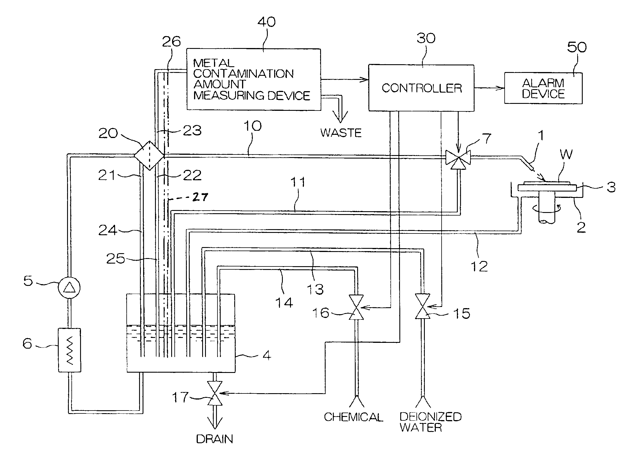
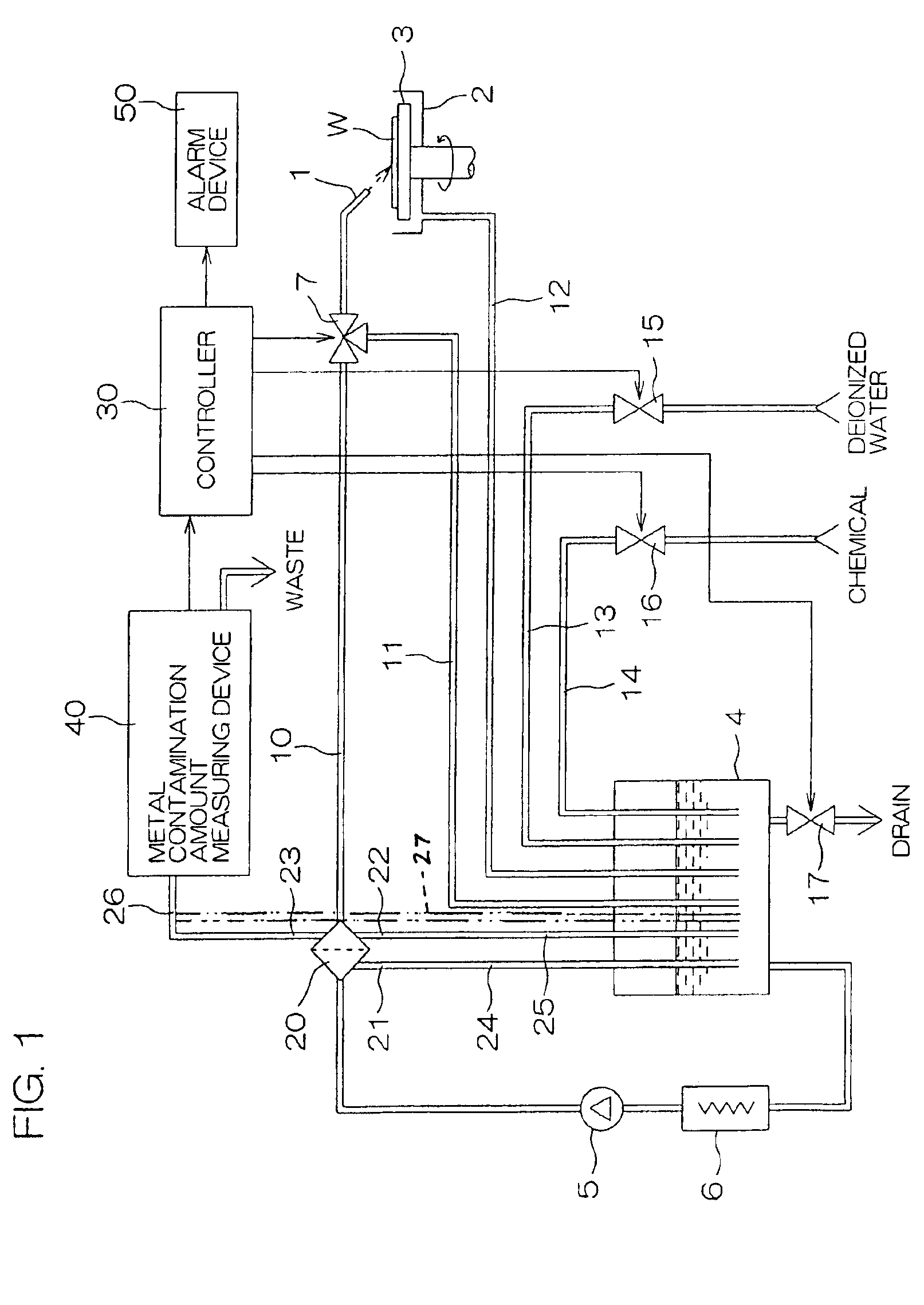
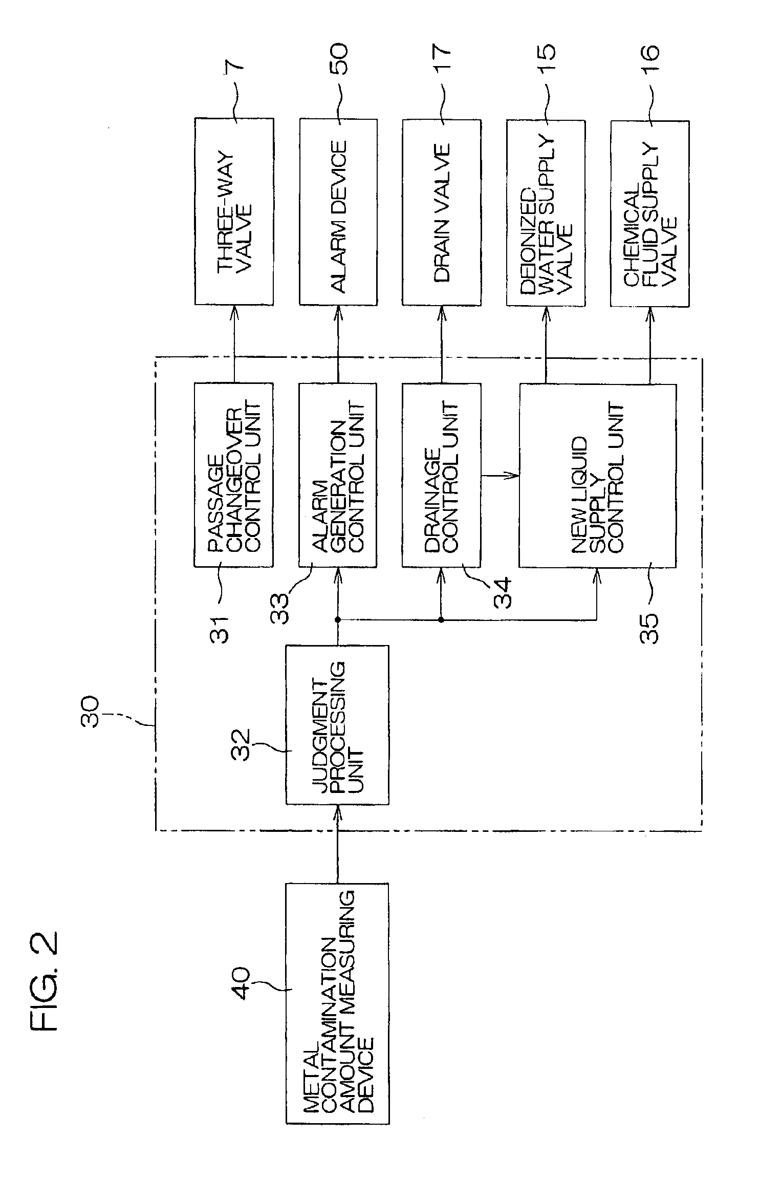
FIG. 1 is a diagram illustrating the arrangement of a substrate processing apparatus according to an embodiment of the present invention. This substrate processing apparatus is arranged to supply a treatment liquid from a treatment liquid supply nozzle 1 onto the surface of a substrate W such as a semiconductor wafer, a liquid-crystal-display glass substrate or the like. Further, this apparatus is of the single-substrate-processing type in which substrates W are processed one by one. More specifically, one substrate W is rotated as held by a spin chuck 3 disposed in a treatment cup 2, and a treatment liquid from the treatment liquid supply nozzle 1 is supplied onto the surface of the substrate W under rotation.

The treatment liquid is stored in a treatment liquid tank 4. Provision is made such that the treatment liquid is pumped out by a pump 5 and supplied to the treatment liquid supply nozzle 1 through a treatment liquid supply passage 10. Disposed along the treatment liquid supply...


PUM

PropertyMeasurementUnit
metallicaaaaaaaaaa
densityaaaaaaaaaa
resistanceaaaaaaaaaa

Abstract

A substrate processing apparatus for supplying a treatment liquid onto the surface of a substrate to treat the same. This apparatus is provided with: a spin chuck for holding and rotating a substrate; a nozzle for supplying a treatment liquid to the substrate held by the spin chuck; a circulating passage arranged such that the treatment liquid supplied to the substrate from the nozzle and used for substrate treatment is circulated to the nozzle and reutilized for substrate treatment; a metal contamination amount measuring device for measuring the metal contamination amount in the treatment liquid passing through the circulating passage; and a judgment processing unit for judging whether or not the value measured by the metal contamination amount measuring device has exceeded a predetermined set value.

Description

BACKGROUND OF THE INVENTION1. Field of the InventionThe present invention relates to substrate processing apparatus for and substrate processing method of supplying a treatment liquid onto the surface of a substrate to treat the same, and more particularly to substrate processing apparatus and method to be applied to a process in which a treatment liquid is contaminated by metal. Examples of a substrate to be treated, include a semiconductor wafer, a liquid-crystal-display-device glass substrate, a plasma-display glass substrate and the like.2. Description of Related ArtHigher-density integration and faster operation of semiconductor integrated circuit elements are the requirements of the marketplace. To meet such requirements, copper wirings lower in resistance are increasingly used instead of conventional aluminium wirings. When a copper wiring is combined with a low-permittivity insulating film (a so-called Low-k film or insulating film made of material of which relative permitti...

Claims


Application Information

Patent Timeline
Patent Type & Authority Patents(United States)
IPC IPC(8): H01L21/00G01N1/32G01N1/28G01N27/48
CPCH01L21/67253Y10S134/902
Inventor OKAMOTO, YOSHIO
Owner DAINIPPON SCREEN MTG CO LTD
Why Eureka
Try Eureka