Systems and methods for characterizing a polishing process

a polishing process and characterization technology, applied in the field of systems and methods for characterizing a polishing process, can solve the problems of over-polishing or under-polishing, current available methods for characterizing, monitoring and/or controlling a cmp process,

Inactive Publication Date: 2005-04-26
KLA TENCOR TECH CORP
View PDF60 Cites 25 Cited by
  • Summary
  • Abstract
  • Description
  • Claims
  • Application Information

AI Technical Summary

Benefits of technology

[0017]In an embodiment, the method may further include dynamically determining a signal threshold distinguishing a presence of the blobs from an absence of the blobs. In such an embodiment, determining if the blobs are present on the specimen may include comparing output signals generated by scanning of the measurement device to the signal threshold to determine if a portion of a blob is present on the measurement spots. In an embodiment, the method may include determining an endpoint of polishing if blobs are not determined to be present on the specimen. The method may also include altering a parameter of the polishing in response to determining an approximate endpoint such that the measurement spots may extend across an area approximately equal to an area of the specimen. For example, a speed of the polishing may be reduced in response to determining the approximate endpoint. The parameter of the polishing may also be altered in response to determining the approximate endpoint to reduce dishing and / or erosion of the specimen.
[0046]A two-dimensional spatially resolved map of characteristics such as metal thickness and optical reflectance values across a specimen provides several advantages over currently available methods of reporting polishing results by annular zones. For example, using such currently available methods, process engineers have no way of inspecting, verifying, and diagnosing wafers that polish in a non-uniform manner. Similarly, the choice of endpoint parameters is haphazard and at best heuristic without taking into account the wafer coverage information that the precession of sensor path determination provides. In addition, process engineers require deterministic methods for setting up, transferring, and modifying polish recipes. Currently available annular zone-based control schemes, however, do not provide such deterministic methods. Furthermore, the effect of de-ionized water provided to a self-clearing objective on the polish process may also be estimated from the precessed sensor path information. This effect may vary by wafer region and by relative rotational speeds of the polishing head and platen. The sensor path determinations provide information about this complicated relationship for the process engineer and aid in fine-tuning polish processes.
[0047]A two-dimensional map of a specimen generated as described herein may provide a two-dimensional computation of specimen surface non-uniformity. Currently available methods use either limited information from a single sensor sweep over the wafer or from merged results within annular specimen “zones.” Such methods are inherently inaccurate because such methods rely on oversampled and averaged data values. Another advantage of the embodiments described herein is that the methods include generating a two-dimensional map of absolute locations of measurement spots on the specimen. For example, a specimen alignment device (or a pre-aligner) of a polishing tool may be configured to detect a notch, flat, or identification mark of a specimen. In this manner, an initial two-dimensional surface map may be generated and oriented to a position of the detected notch, flat, or identification mark. Furthermore, on polishing tools equipped with control mechanisms for altering local polish rates on a specimen, embodiments of methods described herein may provide accurate, two-dimensional non-uniformity parameters, unavailable in currently available methods, by which the polishing process may be controlled as it progresses.
[0052]An embodiment relates to a method for determining a characteristic of a polishing pad. The method may include scanning the polishing pad with a measurement device such as an eddy current device to generate output signals at measurement spots on the polishing pad. The method may also include determining the characteristic of the polishing pad from the output signals. The method may further include determining an approximate lifetime of the polishing pad from the characteristic. The characteristic may include a rate of wear of the polishing pad. In addition, the method may include altering a parameter of a polishing tool in response to the characteristic to reduce the rate of wear of the polishing pad. Furthermore, the method may include altering a parameter of pad conditioning in response to the characteristic.

Problems solved by technology

There are, however, several disadvantages to such currently available methods for characterizing, monitoring, and / or controlling a CMP process.
The polishing-time based method may not effectively handle these changes in the polishing conditions, and thus often produces over-polished or under-polished results.
In addition, measuring monitor wafers reduces production throughput and thus overall equipment efficiency.
Motor current and carrier vibration endpoint detection methods may not provide planarization information in different wafers areas and may not be effective for a shallow trench isolation (STI) process.
There are also, however, several disadvantages to currently available ex situ methods for characterizing, monitoring, and / or controlling a CMP process.
Ex situ methods are also more problematic due to the difficulty of resuming CMP processing of a wafer that is under-polished.
Furthermore, ex situ methods are even more problematic because over-polishing of wafers cannot be actively prevented, only reported after the fact.
Therefore, ex situ process control methods may suffer from a high scrapped wafer rate.
In addition, there are several disadvantages to currently available in situ methods for characterizing, monitoring, and / or controlling a CMP process.
Moreover, indirect monitoring makes process tuning more difficult.
Therefore, these constraints limit the options for CMP processes.
Sometimes such constraints may translate into diminished throughput and polish quality.
Currently available in situ direct methods that use eddy current-based sensors but report only a relative thickness value are known in the art, but a relative process variable is difficult to incorporate into a recipe for transport between process tools.
Moreover, these devices do not compensate for temperature changes that may affect the sensor output.
Currently available methods for whole-wafer measurements of thickness, typically, do not provide spatial resolution.
Therefore, such sensors can only measure one location of the wafer (i.e., the center spot).
Such methods may provide relatively poor performance because the entire wafer does not polish at the same rate as the observed spot.
As such, these techniques provide no method by which to associate a specific spatial location on the wafer with a specific measurement.
This means that CMP defects such as dishing and erosion are likely to be present in this annular zone.
The data processing, however, does not determine where this region lies, except that it is a given distance from the wafer center.
Therefore, annular-zone based measurements provide limited spatial resolution based on the sensor's distance from the wafer center.
However, the annular zone-based information may not be useful since the angular orientation of the wafer is lost in the transfer to the platen used in the second step.
A program of the second control computer may regenerate a full wafer map of surface film features on the wafer, but in the time required to regenerate the map, the wafer may be damaged by over-polishing while these complicated algorithms execute.

Method used


Image

  • Systems and methods for characterizing a polishing process
  • Systems and methods for characterizing a polishing process
  • Systems and methods for characterizing a polishing process

Examples


Embodiment Construction

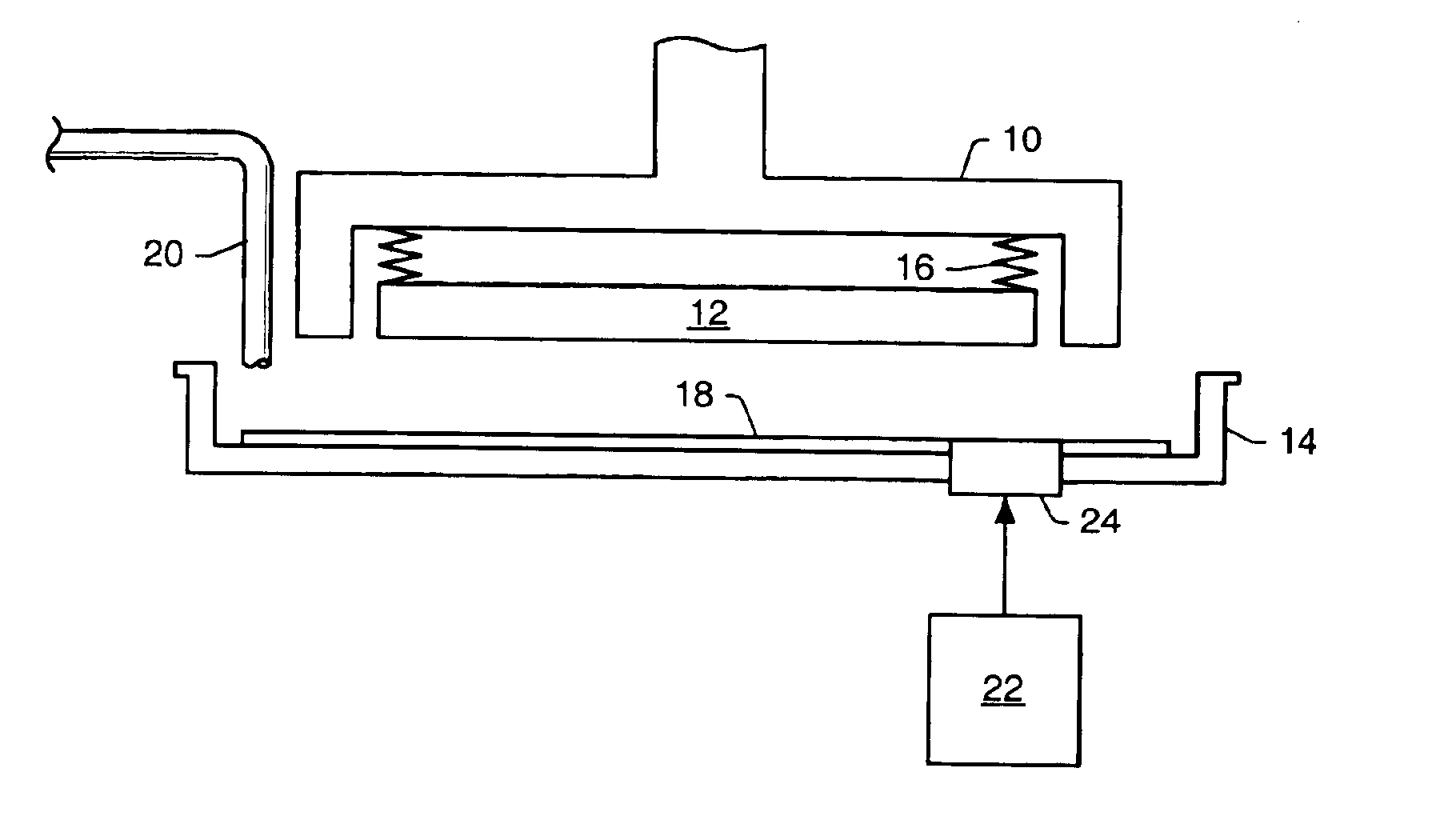
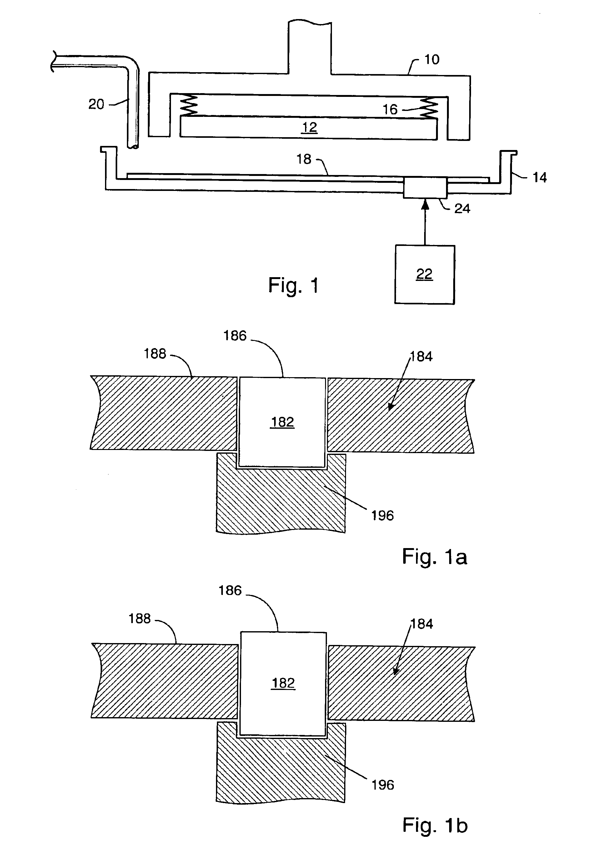
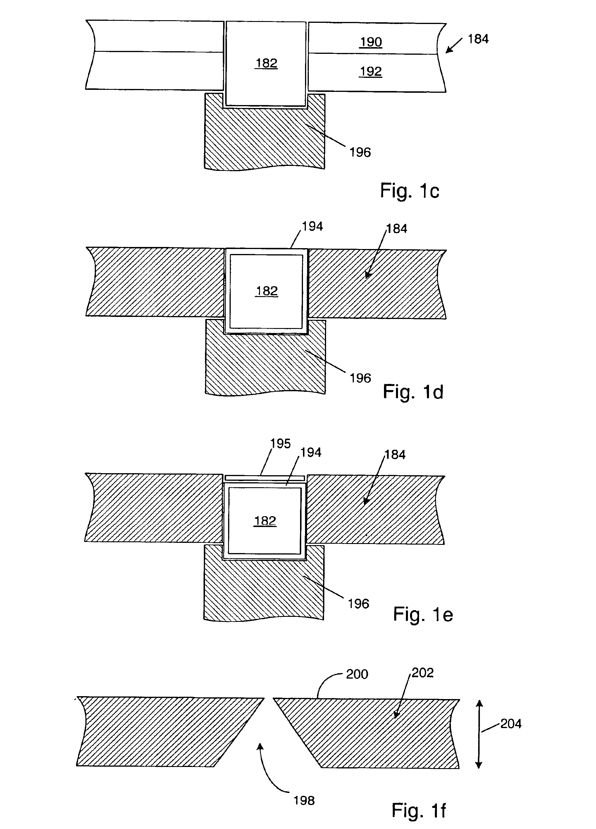
[0079]The following description generally relates to systems and methods for characterizing, monitoring, and / or controlling a polishing process. As used herein, a “specimen” is generally defined to include a wafer or a reticle. The term “wafer” generally refers to substrates formed of a semiconductor or a non-semiconductor material. Examples of such a semiconductor or a non-semiconductor material include, but are not limited to, monocrystalline silicon, gallium arsenide, and indium phosphide. Such substrates may be commonly found and / or processed in semiconductor fabrication facilities.

[0080]A wafer may include one or more layers that may be formed upon a semiconductor substrate. For example, such layers may include, but are not limited to, a resist, a dielectric material, and a conductive material. A resist may include a material that may be patterned by an optical lithography technique, an e-beam lithography technique, or an X-ray lithography technique. Examples of a dielectric ma...


PUM

PropertyMeasurementUnit
thicknessaaaaaaaaaa
thicknessaaaaaaaaaa
thicknessaaaaaaaaaa

Abstract

Systems and methods for characterizing a polishing process are provided. One method includes scanning a specimen with two or more measurement devices during polishing. In one embodiment, the two or more measurement devices may include a reflectometer and a capacitance probe. In another embodiment, the two or more measurement devices may include an optical device and an eddy current device. An additional embodiment relates to a measurement device for scanning a specimen during polishing. The device includes a light source and a scanning assembly. The scanning assembly is configured to scan light from the light source across the specimen during polishing. Another measurement device includes a laser light source coupled to a first fiber optic bundle and a detector coupled to a second fiber optic bundle. An additional method includes scanning a specimen with different measurement devices during different steps of a polishing process.

Description

PRIORITY CLAIM[0001]This application claims priority to U.S. Provisional Application No. 60 / 354,179 entitled “Systems and Methods for Characterizing a Polishing Process,” filed Feb. 4, 2002.BACKGROUND OF THE INVENTION[0002]1. Field of the Invention[0003]The present invention generally relates to systems and methods for characterizing a polishing process. Certain embodiments relate to systems and methods for evaluating optical and / or eddy current data obtained during polishing of a specimen to determine a characteristic of the polishing process.[0004]2. Description of the Related Art[0005]The following descriptions and examples are not admitted to be prior art by virtue of their inclusion within this section.[0006]Fabricating semiconductor devices such as logic and memory devices may typically include processing a specimen such as a semiconductor wafer using a number of semiconductor fabrication processes to form various features and multiple levels of the semiconductor devices. For ...

Claims


Application Information

Patent Timeline
Patent Type & Authority Patents(United States)
IPC IPC(8): B24B37/04B24B49/02B24B49/04B24B49/12B24B49/10B24B41/04
CPCB24B37/013B24B37/042B24B49/12B24B49/04B24B49/10B24B41/04
Inventor LEHMAN, KURTCHEN, CHARLESALLEN, RONALD L.SHINAGAWA, ROBERTSETHURAMAN, ANANTHABEVIS, CHRISTOPHER F.TRIKAS, THANASSISCHEN, HAIGUANGMENG, CHING LING
Owner KLA TENCOR TECH CORP
Why Eureka
Try Eureka