Manufacturing of a low-noise mos device

a transistor and low-noise technology, applied in the direction of semiconductor devices, basic electric elements, electrical appliances, etc., can solve the problems of not addressing the problem of hot-carrier noise and the most common bias situations, and it is practically difficult to achieve a true gradual non-uniform oxide level. , to achieve the effect of low total nois

Inactive Publication Date: 2005-04-26
INFINEON TECH AG
View PDF4 Cites 1 Cited by
  • Summary
  • Abstract
  • Description
  • Claims
  • Application Information

AI Technical Summary

Benefits of technology

[0010]It is an object of the invention to provide a simple method of manufacturing a dual thickness MOS device having a low level of the total noise.
[0030]Thus, for manufacturing an MOS transistor generally the conventional steps of producing a gate oxide layer in a gate oxide region, a source and a drain at the surface of a substrate and a gate located on top of the gate oxide layer are performed, these steps executed in any suitable order. For producing a gate oxide layer having a dual thickness first a thin oxide layer is produced over a portion of the surface of a substrate, preferably by thermal oxidation. A mask layer is applied over the oxide layer and is patterned to form an opening or openings. Then, through the oxide layer in the opening or openings, a material accelerating or retarding the rate of oxidation of the material of the substrate is ion implanted. The mask is thereafter removed, and finally the thermal oxidation over the now totally exposed surface of the thin oxide layer is continued. In the implanted region the oxide layer now formed will be thicker or thinner than the rest of the oxide layer due to the effect of the implanted material.
[0031]The fabrication method has a low complexity and only adds a minimum of processing steps to conventionally used methods of fabricating MOS devices.

Problems solved by technology

As a result of the continuing downscaling of the devices, most of the noise sources of a transistor tend to increase.
However, this never happens and in a real transistor the carriers scatter with various particles like phonons and photons giving a non-uniform velocity distribution.
For minimization of noise created in the device itself, a number of known device and process design tricks can be used, but most of them are not addressing problem of the hot-carrier noise and the most common bias situations.
However, it is practically difficult to obtain a true gradually non-uniform oxide, but a good compromise includes devices having two or three different gate oxide thicknesses.

Method used


Image

  • Manufacturing of a low-noise mos device
  • Manufacturing of a low-noise mos device
  • Manufacturing of a low-noise mos device

Examples


example 1

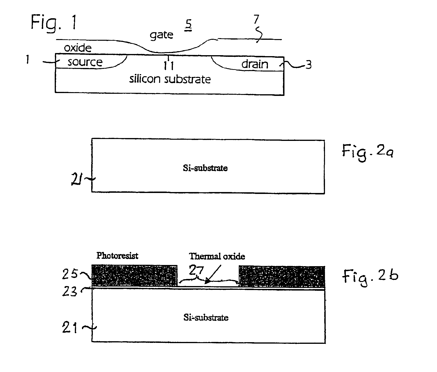
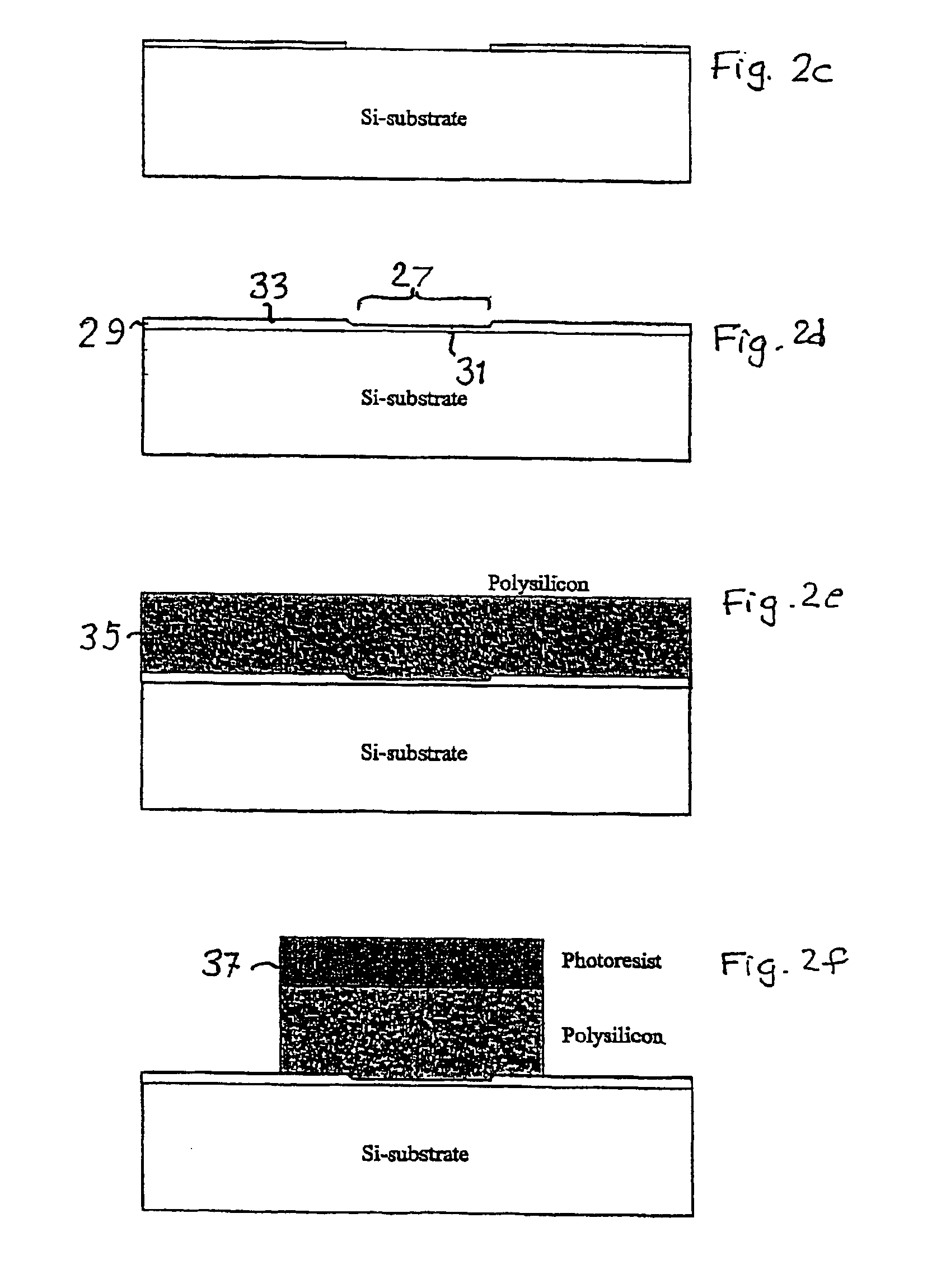
[0048]Fabrication of an MOS transistor using etching to produce two different gate oxide thicknesses will now be described with reference to the schematic cross-sectional views of FIGS. 2a-2g, the production of the dual gate oxide thicknesses being made substantially in the same way as described in the cited U.S. Pat. No. 5,422,505. The device can typically be a 0.5 μm MOS transistor having a gate oxide thickness of 80 and 120 Å The limit will be set by the photolithography in the step illustrated in FIG. 2b, mainly the dimension of the mask relative to the gate length, i.e. to the mask pattern shown in FIG. 2f. The process sequence utilizes no new process steps; all are available in a conventional CMOS process flow. The steps illustrated in FIGS. 2b and 2c have been added to obtain the MOS transistor, these steps including in total the applying of one additional photo mask, one lithographic step, one dry etching step and one gate oxidation step.

[0049]In FIG. 2a the starting materia...

example 2

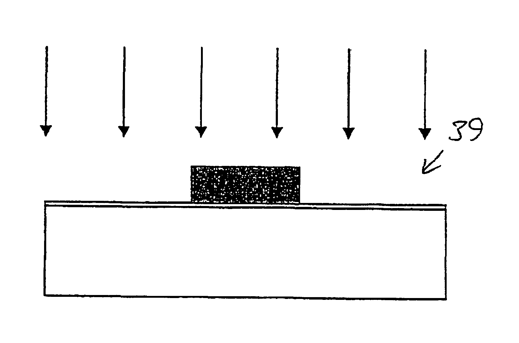
[0058]In a second example, the oxidation rate when producing the thermal gate oxide is enhanced or alternatively retarded by implanting species into the silicon before the final thermal oxidation. Thus for instance, ions, chosen from a group including chloride and bromine ions, are injected to selected areas at the surface of a silicon substrate to increase the oxidation rate of substrate in the implanted areas.

[0059]The steps of the process illustrated by FIGS. 2a-2g, when fabricating a device having two different gate oxide thicknesses using substantially the same parameters as in Example 1, are in this example changed by removing the step of etching a first oxide layer, performed after the step illustrated in FIG. 2b, and instead performing an implanting step illustrated by the schematic cross-sectional view of FIG. 3. In this step a region, which in the figure is an area 39 complementary to the area 27 of e.g. FIG. 2b and which is not covered by the photoresist 25, is implanted ...


PUM


Abstract

At the surface of a substrate a gate oxide layer is produced and is given a dual thickness. A first oxide layer is produced over the surface of a substrate by thermal oxidation and is covered by a mask layer defining suitably located openings. A material accelerating or retarding the oxidation of the substrate is ion implanted through the first oxide layer in the openings, after which the mask is removed and the thermal oxidation is continued over the now exposed total surface of the first oxide layer. The material used for ion implanting can be an oxidation rate promoting material such as chloride and bromine. The manufacturing method is simple and adds little to presently used process flows for fabricating MOS devices. The dual thickness of the gate oxide gives the manufactured MOS device a low level of total noise generated when using the device for instance in RF-circuits.

Description

CROSS REFERENCE TO RELATED APPLICATION[0001]This application is a continuation of copending International Application No. PCT / SE02 / 01380 filed Jul. 12, 2002 which designates the United States, and claims priority to Swedish application no. 0102526-1 filed Jul. 13, 2001.TECHNICAL FIELD OF THE INVENTION[0002]The present invention is related to manufacture of a low noise MOS transistor of interest in CMOS Radio Frequency Integrated Circuit (RF-IC) applications where the noise performance for low-voltage devices is important.DESCRIPTION OF THE RELATED ART[0003]The total noise in any Radio Frequency (RF) circuit is a combination of noise created by different physical phenomena at different locations, see e.g. Chapter 6 in C. D. Motchenbacher, J. A. Connelly, “Low-Noise Electronic System Design”, Wiley, 1997. Usually the dominant noise source is found in the active semiconductor devices. As a result of the continuing downscaling of the devices, most of the noise sources of a transistor te...

Claims


Application Information

Patent Timeline
Patent Type & Authority Patents(United States)
IPC IPC(8): H01L21/02H01L21/28H01L29/423H01L29/40
CPCH01L29/42368H01L21/2822H01L21/28211H01L21/285
Inventor ARNBORG, TORKELJOHANSSON, TED
Owner INFINEON TECH AG
Why Eureka
Try Eureka