Process for producing high quality PZT films for ferroelectric memory integrated circuits

a ferroelectric memory and integrated circuit technology, applied in the direction of transistors, instruments, material analysis, etc., can solve the problems of limiting the life of the system, slow device writing, and limiting the design of some systems

Inactive Publication Date: 2005-05-03
FUJITSU SEMICON LTD
View PDF25 Cites 35 Cited by
  • Summary
  • Abstract
  • Description
  • Claims
  • Application Information

AI Technical Summary

Benefits of technology

[0032]Deposition of the top electrode layer prior to second-stage anneal therefore helps produce high-quality ferroelectric capacitors.
[0033]It has also been found that an alternative process wherein the step of annealing the deposited PZT and the top electrode layer together by RTA is performed after photomasking and etching of the top electrode layer can also produce quality ferroelectric capacitors. Further, alternative processes wherein the step of annealing the deposited PZT and the top electrode layer together by RTA is further delayed until after the passivation layer is deposited and optionally masked, and etched, can also produce quality ferroelectric capacitors.

Problems solved by technology

Standard Dynamic Random Access Memory (DRAM) and Static Random Access Memory (SRAM) devices are considered volatile memory devices because data stored therein is lost when power is lost.
These devices tend to be slow to write-, often having write times on the order of milliseconds, while read times range generally between one nanosecond and one microsecond.
The great difference between read and write times, together with the block-erase character of Flash EEPROM, complicates design of some systems.
CMOS SRAM or DRAM with battery backup power for data retention can provide symmetrical, fast, read and write times in nonvolatile memory but is expensive, requires presence of a battery, and limits system life or requires eventual battery replacement.
It is known that some prior FRAM devices incorporate ferroelectric storage capacitors that degrade with repeated operation, this is known as fatigue degradation.
Some prior FRAM devices incorporate complex circuitry for overcoming fatigue degradation, thereby complicating the design of the device.

Method used


Image

  • Process for producing high quality PZT films for ferroelectric memory integrated circuits
  • Process for producing high quality PZT films for ferroelectric memory integrated circuits
  • Process for producing high quality PZT films for ferroelectric memory integrated circuits

Examples


Embodiment Construction

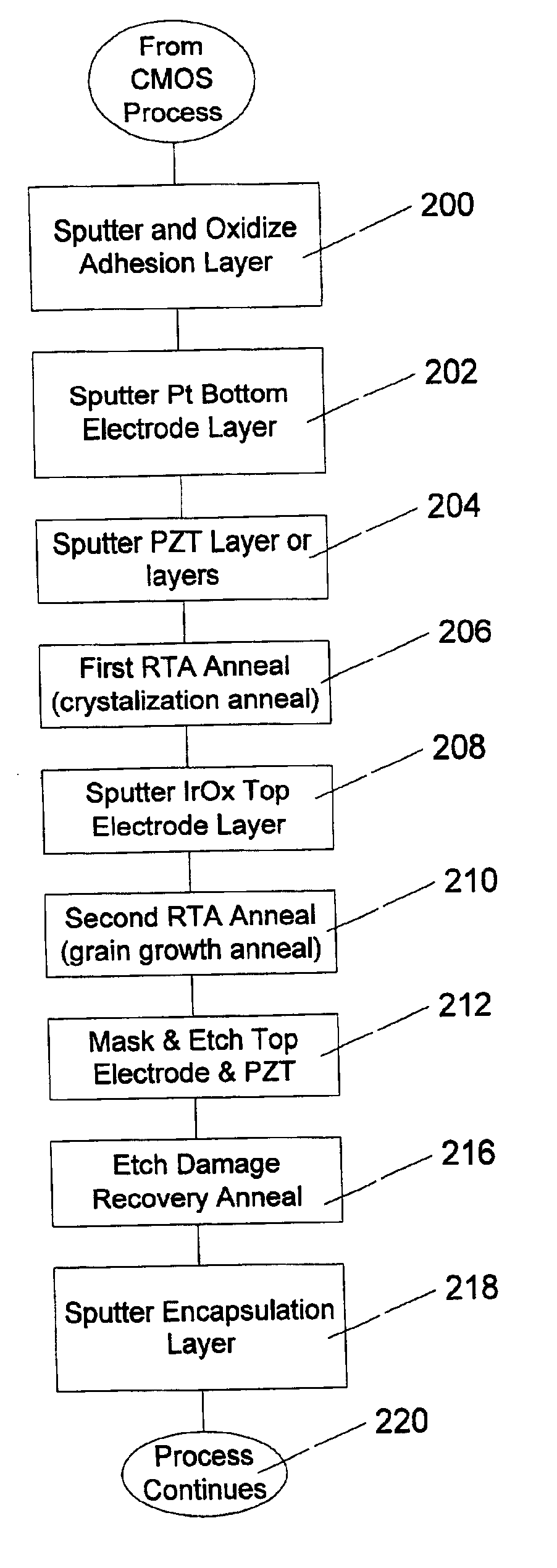
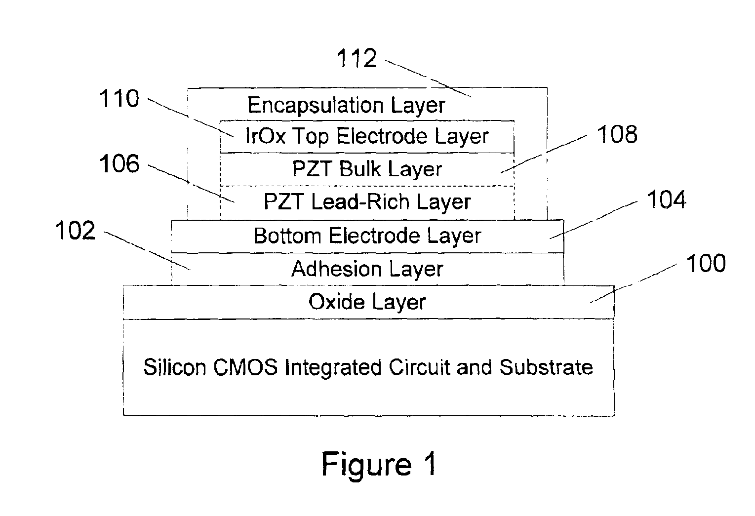
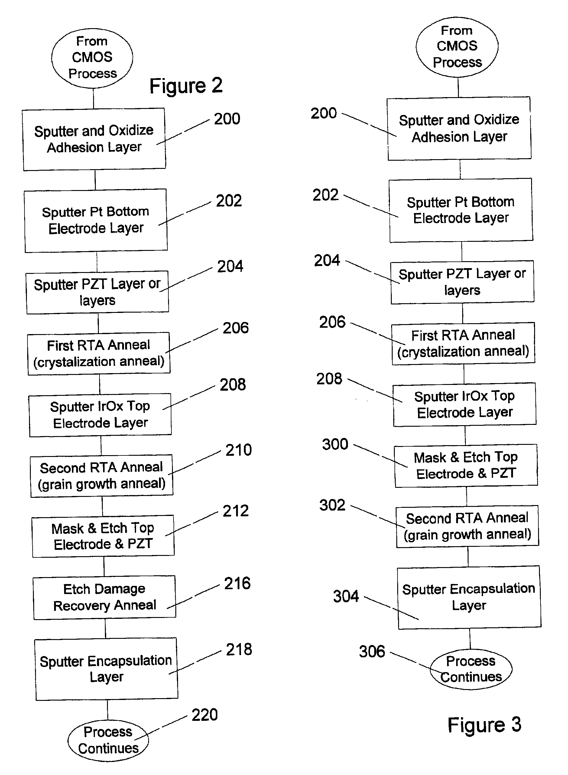
[0039]With reference to FIGS. 1 and 2, a ferroelectric capacitor is typically grown on top of a thermal oxide layer 100 of a partially-finished CMOS integrated circuit wafer. On this oxide layer is sputtered 200 a layer of Titanium from fifty to two hundred, preferably two hundred, angstroms thick. This titanium layer is oxidized at from 300 to 700 degrees C., with 700 degrees C. preferred, for from ten minutes to one hour in oxygen atmosphere to form a adhesion layer 102 of titanium dioxide that enhances adhesion, and thereby prevent delamination, of following layers.

[0040]On the oxidized titanium adhesion layer 100 is sputtered 202 a Platinum bottom electrode layer 104 from 500 to 2500 angstroms thick, with 1000 angstroms thickness preferred for optimum electrode quality. For optimum electrode quality, and optimum quality of following PZT layers, this layer is deposited by DC sputtering with a substrate temperature of 450 to 600 degrees C. For purposes of this application, a noble...


PUM

PropertyMeasurementUnit
partial pressureaaaaaaaaaa
thicknessaaaaaaaaaa
thicknessaaaaaaaaaa

Abstract

A method for fabrication of ferroelectric capacitor elements of an integrated circuit includes steps of deposition of an electrically conductive bottom electrode layer, preferably made of a noble metal. The bottom electrode is covered with a layer of ferroelectric dielectric material. The ferroelectric dielectric is annealed with a first anneal prior to depositing a second electrode layer comprising a noble metal oxide. Deposition of the electrically conductive top electrode layer is followed by annealing the layer of ferroelectric dielectric material and the top electrode layer with a second anneal. The first and the second anneal are performed by rapid thermal annealing.

Description

FIELD OF THE INVENTION[0001]The invention relates to the field of ferroelectric memory integrated circuit processing. In particular the invention relates to deposition and annealing process steps for forming the dielectric and electrode layers of ferroelectric capacitors in ferroelectric memory integrated circuits.BACKGROUND OF THE INVENTION[0002]Standard Dynamic Random Access Memory (DRAM) and Static Random Access Memory (SRAM) devices are considered volatile memory devices because data stored therein is lost when power is lost. Nonvolatile memory devices are those that can retain data despite loss of power.[0003]At present, there is a strong market for EEPROM (Electrically Erasable, Programmable Read Only Memory), and Flash EEPROM nonvolatile memory devices. These devices tend to be slow to write-, often having write times on the order of milliseconds, while read times range generally between one nanosecond and one microsecond. The great difference between read and write times, to...

Claims


Application Information

Patent Timeline
Patent Type & Authority Patents(United States)
IPC IPC(8): H01L21/02H01L21/316H01L21/314H01L27/105H01L21/8246
CPCH01L21/02197H01L21/02266H01L28/56H01L21/31691Y10S438/957H01L27/105
Inventor FOX, GLENCHU, FANEASTEP, BRIANTAKAMATSU, TOMOHIROHORII, YOSHIMASANAKAMURA, KO
Owner FUJITSU SEMICON LTD
Why Eureka
Try Eureka