Method of manufacturing printed-circuit board

a manufacturing method and technology of printed circuit boards, applied in the direction of printed element electric connection formation, insulating substrate metal adhesion improvement, conductive pattern formation, etc., can solve the problems of air bubbles remaining in the filled conductive paste, air bubbles trapped in the conductive paste, interlayer connection resistance may become unstable, water may accumulate in the air bubbles, etc., to reduce the reliability of connection, reduce manufacturing cost, and high density

Inactive Publication Date: 2005-05-10
IBIDEN CO LTD
View PDF23 Cites 82 Cited by
  • Summary
  • Abstract
  • Description
  • Claims
  • Application Information

AI Technical Summary

Benefits of technology

[0053]Laser beam is applied to a glass epoxy substrate of the above thickness range to form a VH. Then, the VH is preferably formed by CO2 laser beam applied under the conditions of pulse energy of 0.5 mJ to 100 mJ, pulse width of 1 μs to 100 μs, pulse spacing of not less than 0.5 ms, and the number of shots of 30 to 50. Further, the bore of the VH is preferably in the range from 50 μm to 250 μm, because in the case of less than 50 μm, the filling of the conductive paste into the VH is difficult, thus reducing the reliability of connection, and in the case of more than 250 μm, it makes higher density difficult.
[0054]Before filling the conductive paste into a VH, de-smear treatment is preferably performed to remove resin residues remaining on the inner wall of the VH in the light of ensuring connection reliability. Therein, for example, either of a dry de-smear treatment using plasma discharge or corona discharge, and a wet de-smear treatment using potassium permanganate solution and the like may be used. After the de-smear treatment on the VH in the above-described insulating substrate, a vacuum pressure degassing method is used to fill the VH with the conductive paste, which method is suitable for reducing the manufacturing cost and increasing the yield.
[0055]Further, the above-described plasma cleaning is preferably performed under the conditions of the output, degree of vacuum, reacting gas species, and energizing time such that the temperature of the circuit board may be kept below 60° C. The de-smear treatment by plasma cleaning can remove resin residues remaining in a VH without damaging the PET film and resin bonding-agent, which treatment is in synergy with the filling of the conductive paste by vacuum pressure degassing to permit interlayer connection resistance to be stabilized. For the plasma cleaning, the insulating substrate provided with a VH is placed on an electrode provided in the chamber of a known plasma cleaning apparatus, with the opening directed upward. Thus, the plasma cleaning is preferably performed with the electrode itself cooled such that the temperature of the bonding agent layer bonding copper foil to the insulating substrate and the temperature of the bonding agent layer and protective film bonded to the insulating substrate in the step of laser beam machining may be lower than the softening temperature of these resins. For this purpose, the conditions of the output, degree of vacuum, reacting gas species, and energizing time should be appropriately selected. By such treatment, resin residues can be plasma-cleaned and also it is possible to prevent the displacement of an opening and the peeling of the protective film caused by the softening of the resin bonding-agent. In this case, the insulating substrate is more advantageously placed on the electrode in the chamber via a heat-conductive sheet made of silicone resin containing metal particles, such that the substrate can more effectively dissipate the heat received thereby to the electrode.
[0056]Further, the thickness of the copper foil is desirably 3 μm to 18 μm and the hot-press is performed under appropriate temperature and applied pressure. The hot-press is more preferably performed under a condition of reduced pressure such that only the resin bonding-agent layer in the half-cured state may be cured, thereby permitting the copper foil to be strongly bonded to the insulating substrate. Thus, the manufacturing time can be reduced rather than that of the conventional circuit board using preapreg.

Problems solved by technology

In the filling of the paste by such methods, there has been a problem that air bubbles may be trapped into the conductive paste during the agitating or printing described above.
This problem is remarkable in the filling of a highly-viscous conductive paste containing much conductive filler, then resulting in air bubbles remaining in the filled conductive paste.
When the paste is cured in the state of still containing air bubbles, fears are in that the interlayer connection resistance may become unstable and / or water may be accumulated in the air bubbles.
Particularly, if the paste retains moisture, there is the risk of a water vapor explosion under a high temperature atmosphere in reflow soldering process.
Further, the larger the amount of conductive filler contained in such conductive paste is, the higher the viscosity of the paste is.
However, air is easily involved into the paste during kneading and filling, thereby resulting in a problem that air bubbles are easy to remain in the filled conductive paste.
On the other hand, when a low viscous paste containing relatively small amount of conductive filler is filled into an opening, the involving of air into the paste during kneading and filling is reduced, but there is a problem that the resultant depression on the surface is large in depth.
If air bubbles remain in the filled paste, they may contain moisture.
In this case, after incorporated into electronic parts, the air bubble-containing paste may cause delamination in heat treatment such as reflow soldering, thereby resulting in degradation in connection resistance.
Further, if the depression on the surface is large in depth, the filled conductive paste can not be sufficiently compressed during lamination press.
That is, although the conductive paste is depressed downward by the thickness of the bump, the amount of depression is so small that the conductive filler can not closely contact with each other, thus easily causing a problem of degradation in connection resistance.
When a conductive paste in the center of VH's is also scraped off by a squeeze in the stage of squeezing treatment in printing and filling the conductive paste into the interior of the VH's, the problem concerning a depression in the surface can occur.
Further, when the conductive paste contains volatile solvent components in large amount, the volume of the conductive paste reduces in the stage of pre-curing the conductive bump, thus causing a similar problem.
However, because conventional conductive pastes do not satisfy the above properties, they can not be used for manufacturing the conductive bumps.
However, in the manufacturing process of the multilayer circuit boards having the above-described IVH structure, there have been problems caused by an uncured resin used as an insulating resin substrate, such as glass epoxy preapreg obtained by impregnating glass fabric with a epoxy resin.
In order to deal with such displacements, the diameter of via lands has been required to be made large in advance, thereby making precision wiring difficult.
However, this proposal has the following problem to be solved.
Therefore, there remains a realistic problem of the increased cost of manufacturing of the multilayer circuit board.

Method used


Image

  • Method of manufacturing printed-circuit board
  • Method of manufacturing printed-circuit board
  • Method of manufacturing printed-circuit board

Examples


first embodiment

(First embodiment)

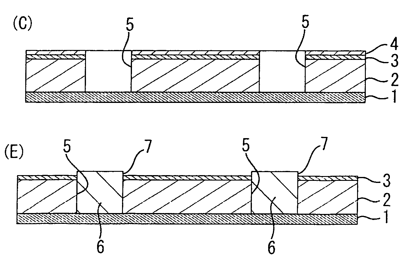
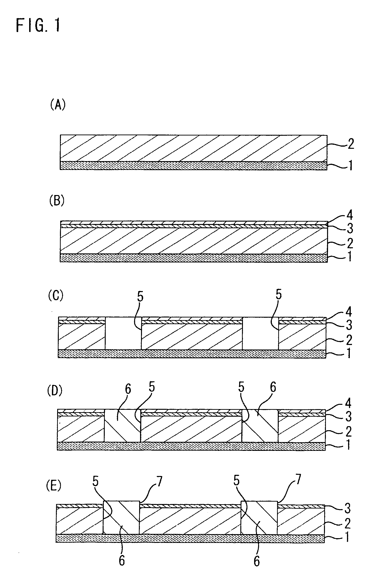
[0069]Next, the first embodiment of the present invention will be described with reference to FIG. 1 to FIG. 4.

[0070](Preparation of conductive paste)

[0071]As a conductive filler, 100 weight parts of flake-like silver having an average particle diameter of 10 μm were used. For a binder, 3.2 weight parts of a novolac epoxy resin having a molecular weight of 600 and 3.2 weight parts of a phenolic plastic having a molecular weight of 10000 to 15000 were used as thermosetting resins, and 6.8 weight parts of ethyl carbitol acetate were used as a solvent. The binder was prepared by mixing together the novolac resin and phenolic plastic, which are both solid at room temperature, and adding the ethyl carbitol acetate to dissolve the resins. The resultant matter obtained by adding and mixing silver to this binder was used as a conductive paste.

[0072]When conventional liquid epoxy resins of low molecular weight are subjected to pre-cure treatment, they start a cross-link re...

second embodiment

(Second embodiment)

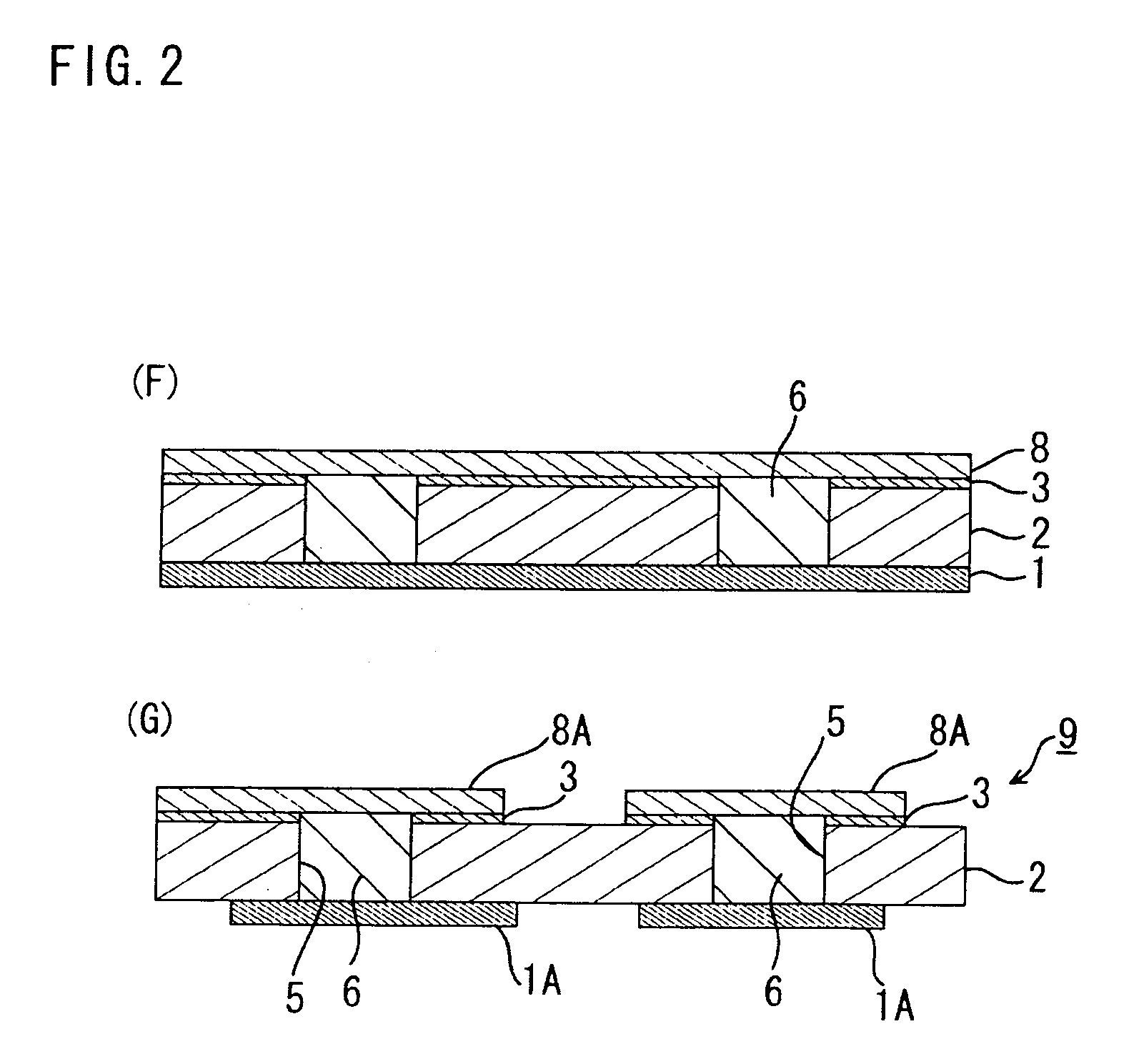
[0089]In stead of the conductive paste 6 described in the first embodiment, two kinds of conductive pastes of low viscosity and of high viscosity can be used to fill the VH. Hereinafter, it will be described how this method is used to manufacture a multilayer wiring board. For example, as a low-viscosity conductive paste, a paste containing a filler of silver-plated copper particles and having a viscosity of 0.9 Pa·s is injected into an opening up to the height of 2 / 3 of a VH diameter, wherein the opening is for forming the VH and is formed by laser beam machining, such as the VH 5 shown in FIG. 1(C) or FIG. 3(D). Further, as a high-viscosity conductive paste, a paste containing a filler of silver-plated copper particles or silver particles and having a viscosity of 4 Pa-s is successively filled into the opening by using a metal mask having an opening diameter of 200 μm and a thickness of 100 μm, stacking over the low-viscosity conductive paste, thus forming VH. A...

third embodiment

(Third embodiment)

[0093]The third embodiment will be described with reference to FIG. 5 to FIG. 6.

[0094]Copper foil 102, for example, is provided on the whole underside of an insulating substrate 104 for forming a circuit board 101 (FIG. 5(A)). Further, after forming a conductive bump 103, this copper foil 102 is etched to form a conductor circuit. As shown in FIG. 5(B), two sheets of peeling coatings 105 and 106 are bonded on the upper surface of this insulating substrate 104 (by the way, hereinafter, a peeling coating of the upper side 105 is referred to as a first peeling coating 105 and a peeling coating of the lower side 106 is referred to as a second peeling coating 106). Both peeling coatings 105 and 106 are made of PET. Although not shown in detail, the undersides of both peeling coatings 105 and 106 are provided with an adhering agent layer.

[0095]Next, a VH 107 is formed at a predetermined position by a CO2 laser (FIG. 5(C)). The VH 107 passes through both peeling coatings...


PUM

PropertyMeasurementUnit
glass transition temperatureaaaaaaaaaa
viscosityaaaaaaaaaa
viscosityaaaaaaaaaa

Abstract

By filling a predetermined amount of conductive paste into an opening for forming a through hole or a VH formed in a resin insulating layer of a circuit board, and pressurizing the filled conductive paste under the condition of reduced pressure, removing air bubble strapped in the conductive paste.

Description

TECHNICAL FIELD[0001]The invention relates to a method for manufacturing printed wiring boards (which may be referred to as “circuit boards” in the present specification), which method is particularly suitable for manufacturing multilayered printed-wiring boards.BACKGROUND ART[0002]In the manufacturing of circuit boards, the following methods have been generally used to fill electrically conductive paste into penetrations for through holes and openings for via holes (VH) in the circuit boards. First, conductive filler and resin particles are added to conductive metal particles, the resultant of which is mixed into solvent to make a mixture, and then the mixture is agitated into a conductive paste. Thereafter, a mask is placed on the penetration or opening positions, and then, from the top of the mask, the conductive paste is filled into the penetrations or openings with a squeegee by the method of printing. Alternatively, another method directly fills the conductive paste into the p...

Claims


Application Information

Patent Timeline
Patent Type & Authority Patents(United States)
IPC IPC(8): H05K3/40H05K3/46H05K3/38
CPCH05K3/4069H05K3/386H05K3/4614H05K2201/0355H05K2201/0394Y10T29/49165H05K2203/0278H05K2203/085H05K2203/1461Y10T29/49155Y10T29/49117H05K2203/0191
Inventor ENOMOTO, RYOKARIYA, TAKASHISAKAMOTO, HAJIME
Owner IBIDEN CO LTD
Why Eureka
Try Eureka