
Vertical cavity surface emitting laser and a method of fabrication thereof

a laser and laser technology, applied in the direction of laser optical resonator construction, laser details, nanooptics, etc., can solve the problems of low yield, difficult to achieve dbr based mirrors with high reflectivity, complicated processing schemes, etc., to achieve simple fabrication of the device according to the invention, good thermal conductivity, and high structural quality

Inactive Publication Date: 2005-05-10
ECOLE POLYTECHNIQUE FEDERALE DE LAUSANNE (EPFL)
View PDF4 Cites 6 Cited by
  • Summary
  • Abstract
  • Description
  • Claims
  • Application Information

AI Technical Summary

Benefits of technology

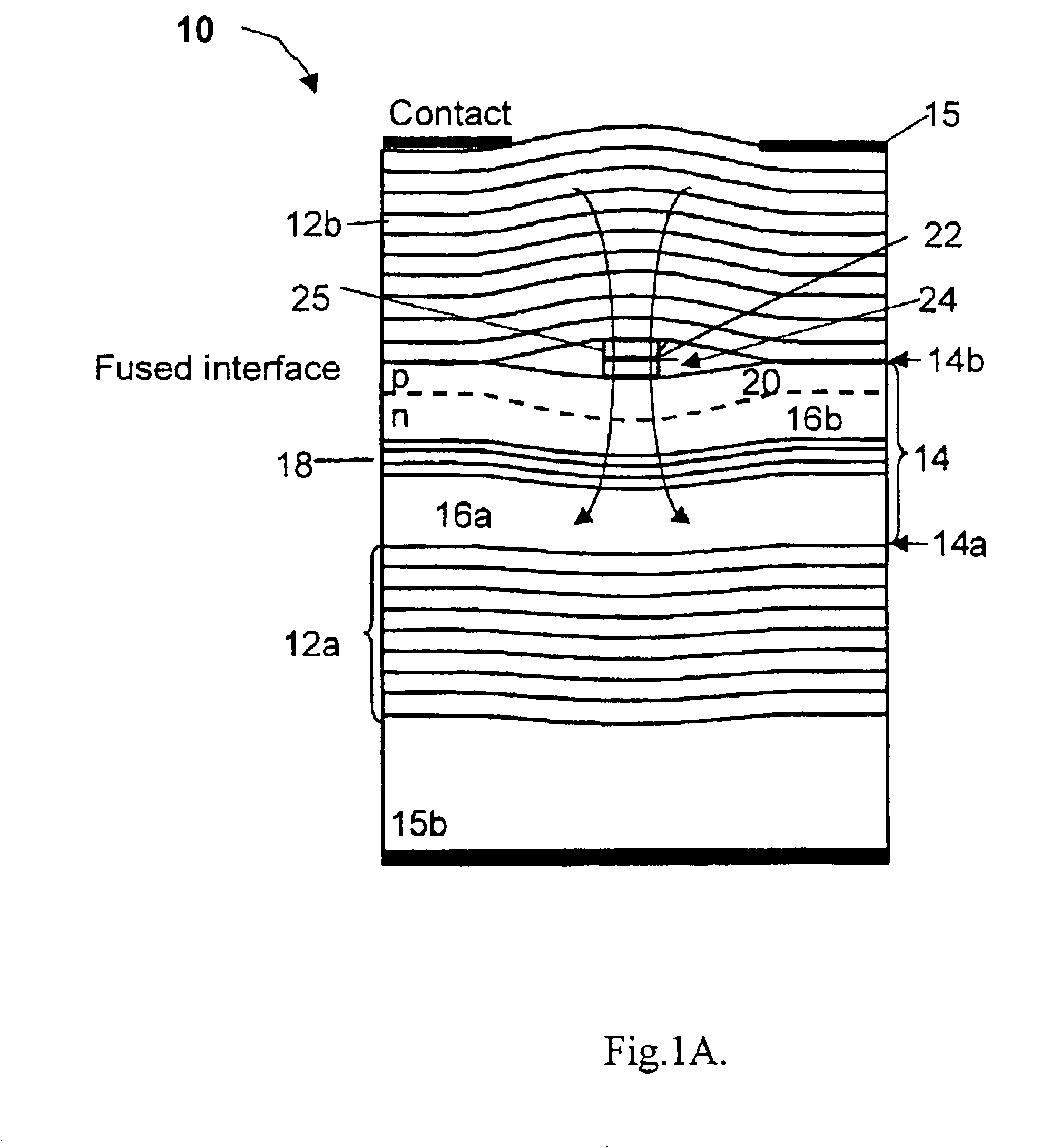
[0014]The main idea of the present invention consists of the following. A VCSEL device structure that includes an active cavity material sandwiched between two DBRs is formed with an active region defined by an aperture between a structured surface of the active cavity material and a substantially planar surface of a n-type layer of one of the DBRs, the structured surface and the planar surface of the n-type layer being fused to each other. The structured surface is formed by a top surface of a mesa, which includes at least an upper n++ layer of a p++ / n++ tunnel junction formed on top of a p-semiconductor layer which is part of the active cavity material, and a top surface of a p-type layer (i.e., either the p++ layer of the tunnel junction, or the p-semiconductor layer, as the case may be) outside the mesa. The structured surface (i.e., both the upper surface of the mesa and the surface of the p-type layer outside the mesa) is fused to the planar surface of the n-type layer of the DBR, as a result of deformation of these surfaces. As a consequence, an air gap is formed in the vicinity of the mesa between the fused surfaces, presenting the aperture between the fused surfaces. This allows for restricting an electrical current flow to the active cavity material (i.e., the formation of the current aperture which defines the active region), and for lateral variation of the index of refraction within the active region.
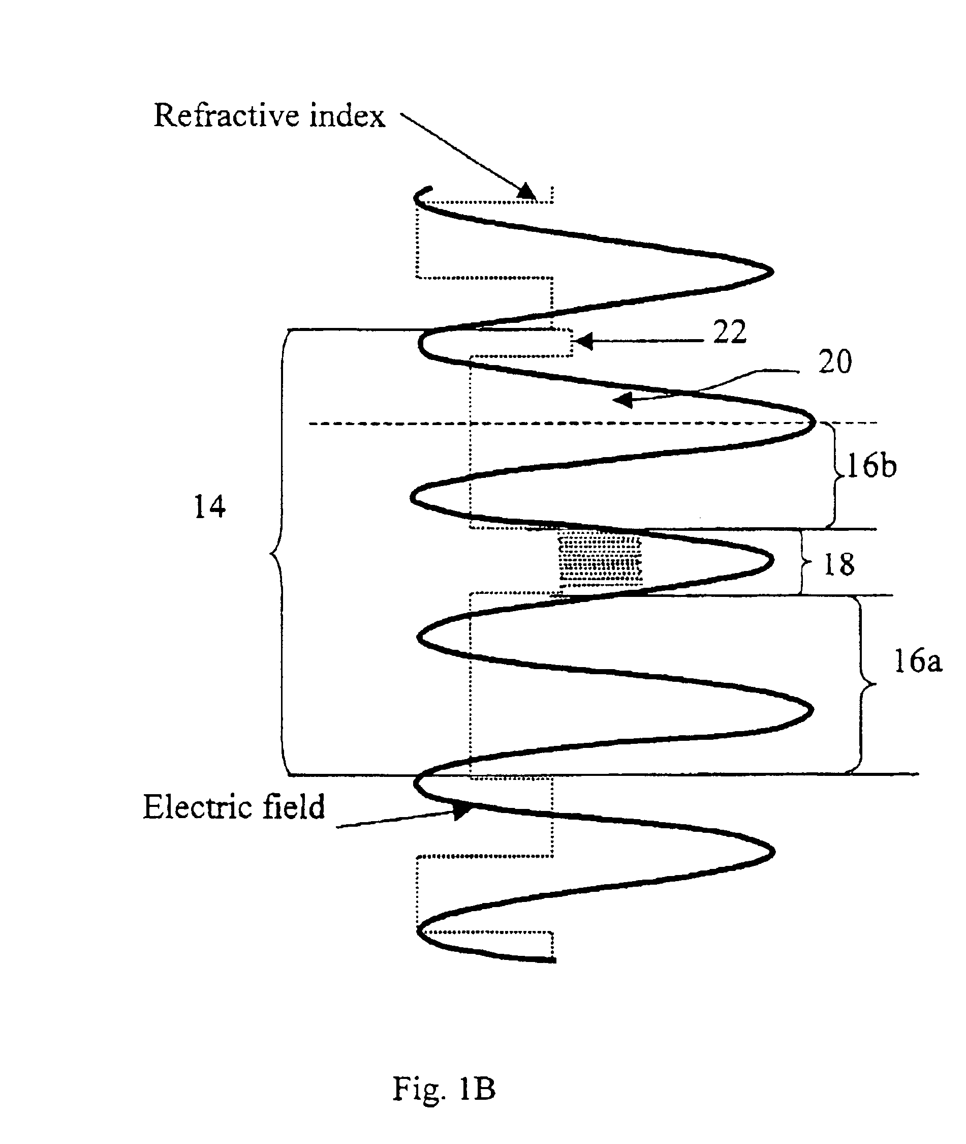
[0017]Thus, according to the technique of the present invention, a mesa is formed in the tunnel junction (a stack of p++ and n++ layers) on top of a p-layer which is part of the active cavity material, and the wafer fusion is applied between a lower n-type planar layer of the DBR and the structured surface of the active cavity material. This process, due to deformation of the wafers (DBR structure and the active cavity material structure), results in a specific topology of the layers around the mesa and in the creation of an air gap defined by the height of the mesa and the pressure applied at fusion temperature. The provision of the air gap allows for the lateral refractive index variation in the active region of the device. The provision of an electric field directed from top to bottom causes both the tunnel junction in the mesa and the n-p (or n-p++) fused interface to be reversed biased, thereby restricting the current flow through the mesa.
[0028](iii) applying a wafer fusion between the structured surface of the active cavity material and a substantially planar surface of a n-type semiconductor layer of a first distributed Bragg reflector (DBR) stack, thereby causing deformation of the fused surface around the mesa and defining an aperture region for electrical current flow therethrough, the aperture region including the mesa surrounded by an air gap between the deformed fused surfaces and defining an active region of the device;
[0032]Distinguished from the known techniques of fabricating long wavelength VCSELs based on the tunnel junction approach, the technique of the present invention allows using a high structural quality AlAs / GaAs DBR with very good thermal conductivity. Both lateral electrical and optical confinements are obtained while performing the fusion of the AlAs / GaAs DBR to the active cavity material with a low resistivity n++InP-based / n-GaAs fused junction.
[0033]It should be noted that the method of fabrication of the device according to the invention is simple, does not include any non-standard process, and allows the fabrication of multiple wavelength VCSEL arrays. The final device is mechanically stable allowing a large scale and low cost production.

Problems solved by technology

In this system, however, it is practically Impossible to achieve DBR based mirrors with-high enough reflectivity because of the small difference in the refractive indices in this material system.
However, this approach leads to a non-planar structure, since mesa etches are required, resulting in a complicated processing scheme and low yield.
The lateral oxidation is very sensitive to various factors like temperature, surface quality and defects, and does not allow obtaining current apertures with a precise size, and, above all, uniform enough to be used in the fabrication of multiple wavelength arrays by cavity length engineering.
In case of lateral oxidized devices, it is quite difficult to use high performance AlAs / GaAs DBRs with highest refractive index contrast and best thermal characteristics, as compared to other AlGaAs / GaAs DBRs.
This approach, however, suffers from the following drawbacks: the fused p-GaAs-based and p-InP-based interfaces are normally highly resistive resulting in a substantial heating of the device; and it is very difficult to optimize p-AlGaAs / GaAs DBRs for long wavelength VCSELs to have both high reflectivity (low absorption) and low resistivity.
Besides the above-mentioned drawbacks related to this particular lateral confinement technique and to highly resistive p-GaAs / p-InP fused junctions, this approach suffers from the known difficulty in obtaining low resistive reversed biased tunnel junctions in GaAs, as compared to lower band-gap materials.
However, an oxide DBR with intrinsically low thermal conductivity is placed between the active region and the heat-sink.
The final device represents a free standing epitaxial structure without a substrate, thereby adding complexity in handling and processing such devices and reducing the yield.
However, such a structure is characterized by the lattice mismatch of 3.7% between GaAs-based and InP-based compounds, resulting in a high density of defects in the metamorphic AlGaAs / GaAs DBR.
These defects propagate into the active region which may result in a fast degradation of the device.
The proton implantation also creates defects and especially in the InP-based active cavity material.
Additionally, the resulting structure does not comprise a means for lateral optical confinement.
The disadvantage of this device structure is that it also does not include a means for lateral optical confinement.

Method used


Image

  • Vertical cavity surface emitting laser and a method of fabrication thereof
  • Vertical cavity surface emitting laser and a method of fabrication thereof
  • Vertical cavity surface emitting laser and a method of fabrication thereof

Examples


Embodiment Construction

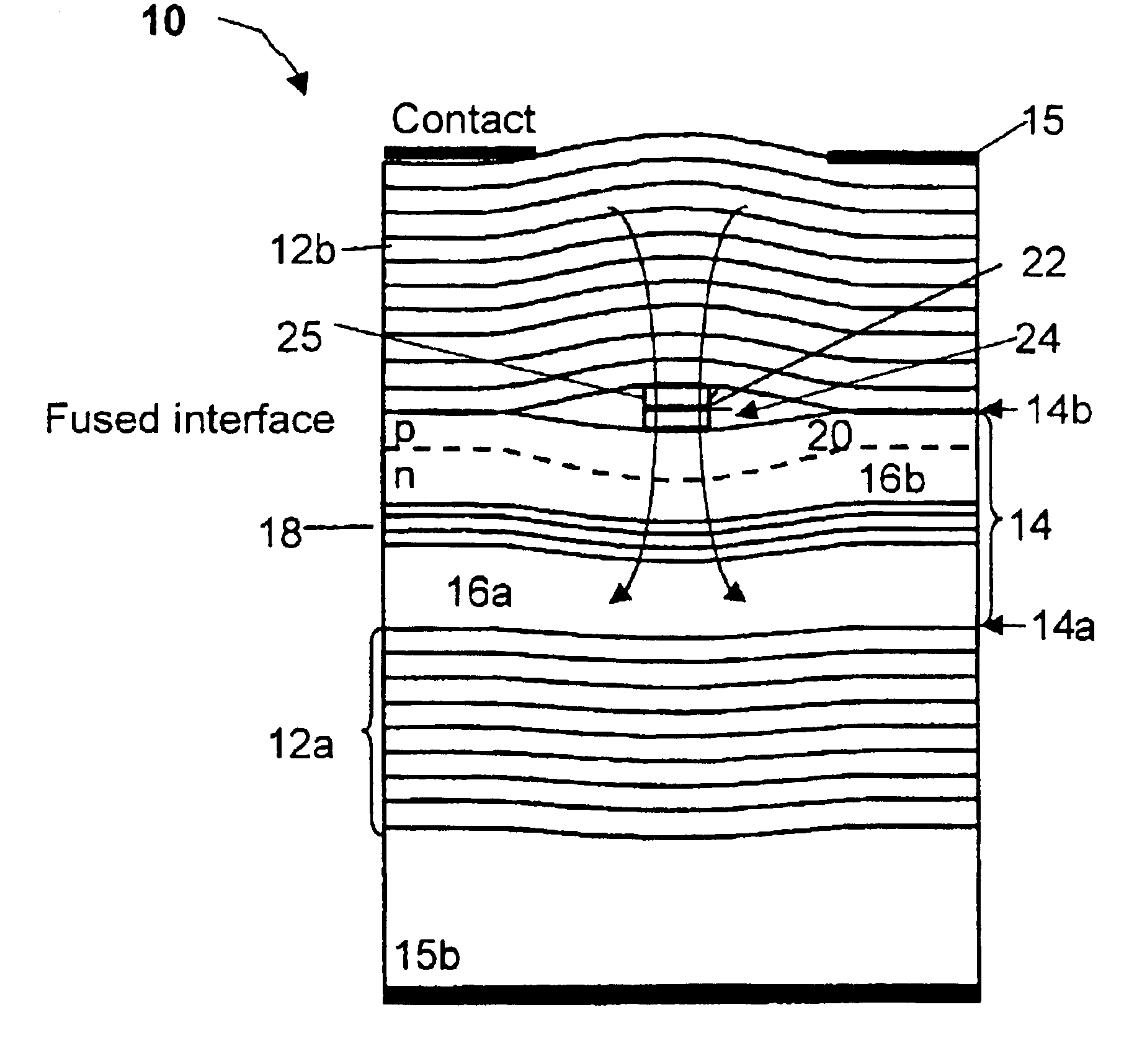
[0043]FIG. 1A illustrates a VCSEL device structure, generally designated 10, according to one embodiment of the present invention. The device 10 is composed of bottom and top n-AlAs / GaAs DBRs 12a and 12b, and an active cavity material, generally at 14, therebetween. The DBRs 12a and 12b are bonded to, respectively, a bottom surface 14a and an upper, structured surface 14b of the active cavity material 14, by wafer fusion. Ohmic contacts, generally at 15, are provided on opposite sides of the device 10.

[0044]The active cavity material 14 is a structure incorporating a bottom n-type spacer 16a, a multi-quantum well (MQW) structure 18, a top spacer 16b terminating with a p-type layer 20, and a mesa 22, which is p++ / n++ tunnel junction composed of a p++ bottom layer and a top n++ layer. Hence, the structured surface 14b is formed by the upper surfaces of the mesa 22 and of the p-type layer 20 outside the mesa 22. The lower surface of the n-type DBR 12b (i.e., of the n-semiconductor laye...


PUM


Abstract

An electrically pumped VCSEL and a method of its fabrication are presented. The VCSEL comprises an active cavity material sandwiched between top and bottom DBR stacks, the top DBR having at least one n-semiconductor layer. The device defines an aperture region between the structured surface of the active cavity material and the n-semiconductor layer of the top DBR stack. The structured surface is formed by a top surface of a mesa that includes at least the upper n++ layer of a p++ / n++ tunnel junction and the surface of a p-type layer outside the mesa. The structured surface is fused to the surface of the n-semiconductor layer of the DBR stack due to the deformation of these surfaces, thereby creating an air gap in the vicinity of the mesa between the fused surfaces. The active region is defined by the current aperture which includes the mesa surrounded by the air gap, thereby allowing for restricting an electrical current flow to the active region, while the air gap provides for the lateral variation of the index of refraction in the VCSEL.

Description

CROSS-REFERENCE TO RELATED APPLICATIONS[0001]This application is a divisional application of PCT / IB02 / 00683 filed on Mar. 8, 2002 and of U.S. Ser. No. 09 / 809,239 filed on Mar. 15, 2001, now U.S. Pat. No. 6,542,531 all of the same title, the applications having common inventors, and the contents of which being incorporated herein by reference thereto. Priority under 35 U.S.C. §119 is claimed to these prior applications.FIELD OF THE INVENTION[0002]This invention relates to vertical cavity surface emitting lasers (VCSELs), and particularly to electrically pumped, long wavelength VCSELs and multiple wavelength VCSEL arrays, and a method of fabrication thereof.BACKGROUND OF THE INVENTION[0003]A VCSEL is a semiconductor laser including an active region sandwiched between mirror stacks that can be semiconductor distributed Bragg reflectors (DBRs) [N. M. Margalit et al., “Laterally Oxidized Long Wavelength CW Vertical cavity Lasers”, Appl. Phys. Lett., 69 (4), Jul. 22 1996, pp. 471-472], or...

Claims


Application Information

Patent Timeline
Patent Type & Authority Patents(United States)
IPC IPC(8): H01S5/00H01S5/183H01S5/10
CPCB82Y20/00H01S5/18308H01S5/18316H01S5/18341H01S5/18358H01S5/423H01S5/18388H01S5/2063H01S5/3095H01S5/34306H01S5/4087H01S5/1838
Inventor KAPON, ELYAHOUIAKOVLEV, VLADIMIRSIRBU, ALEXEIRUDRA, ALOK
Owner ECOLE POLYTECHNIQUE FEDERALE DE LAUSANNE (EPFL)
Learn More