

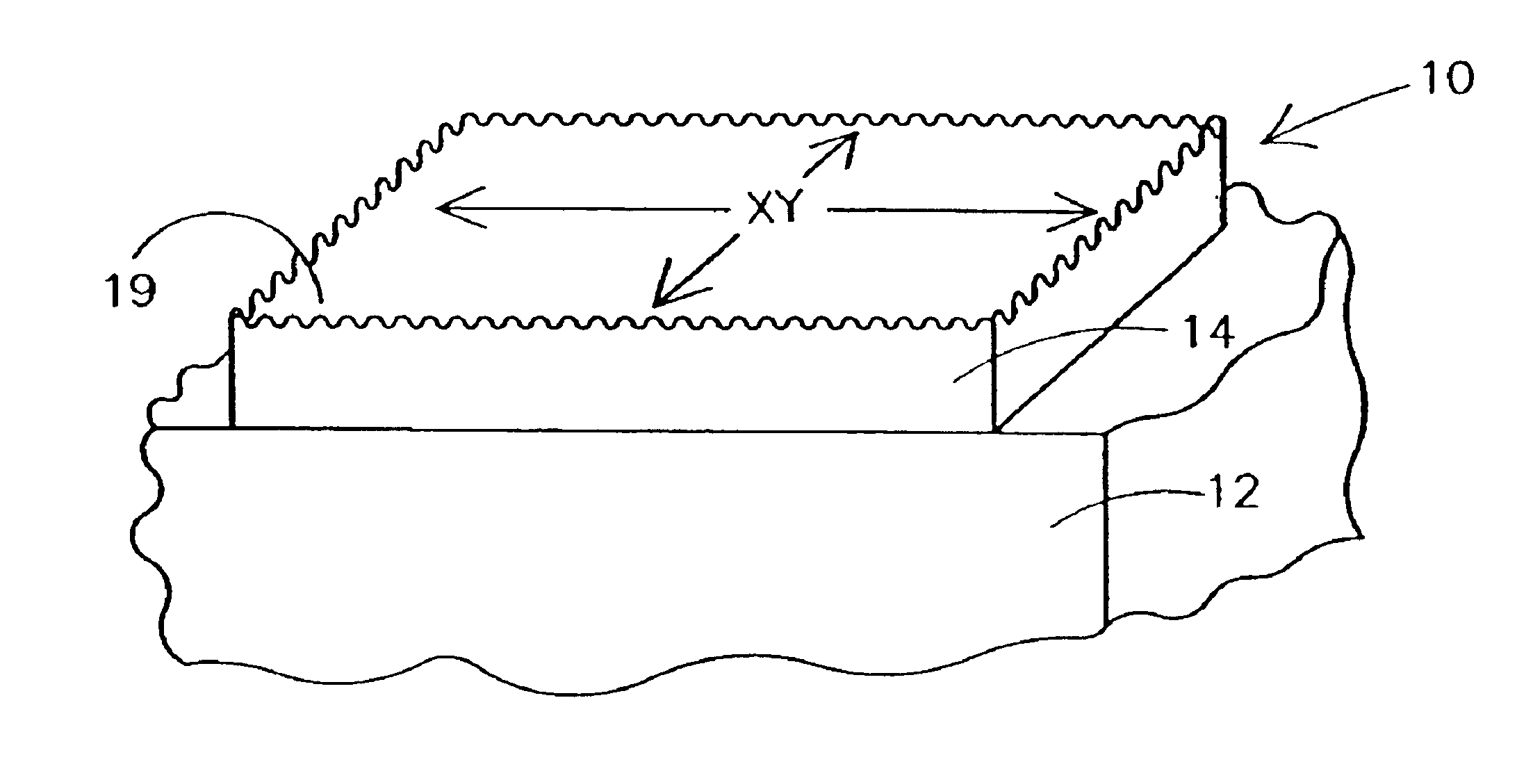
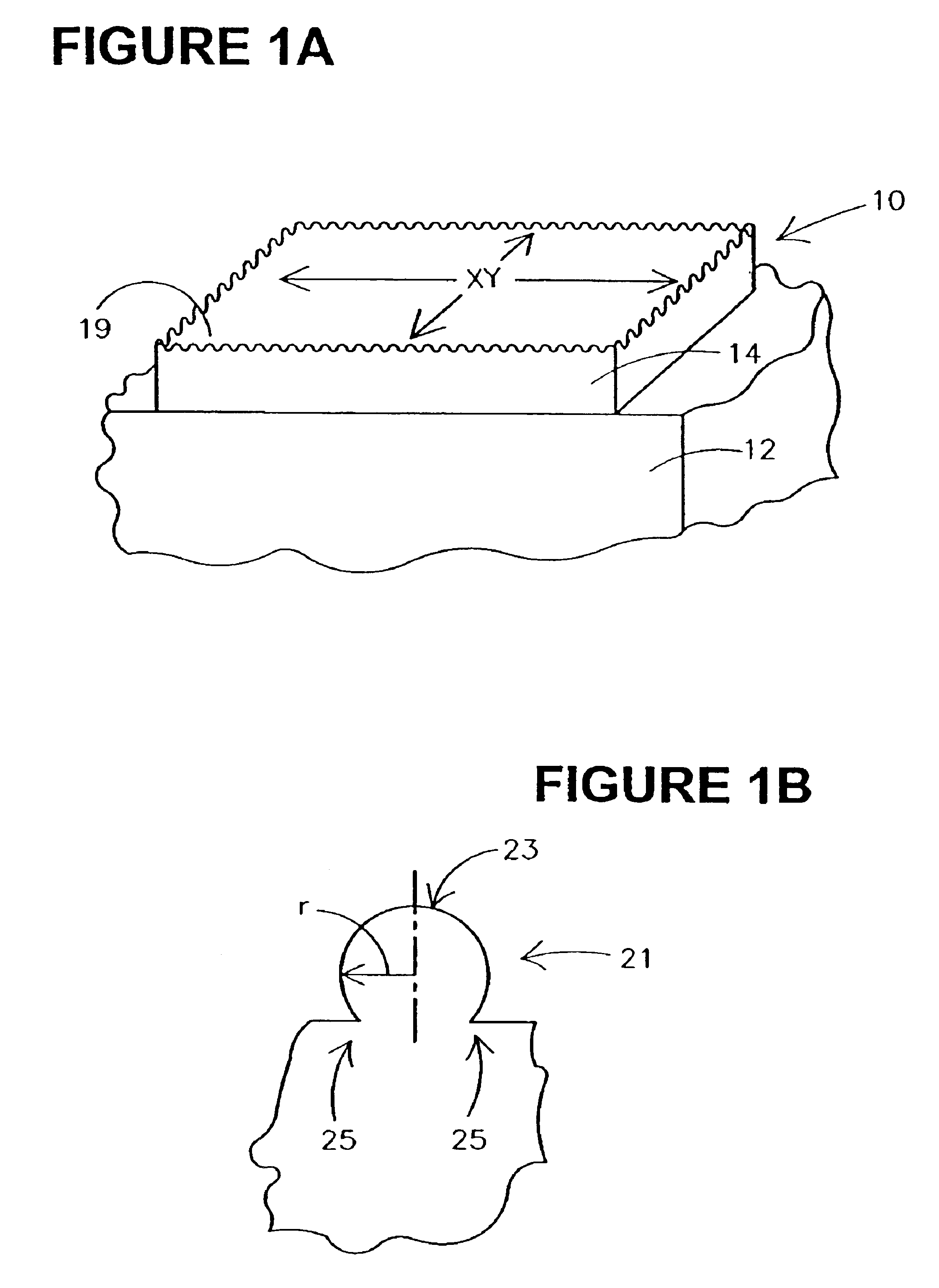
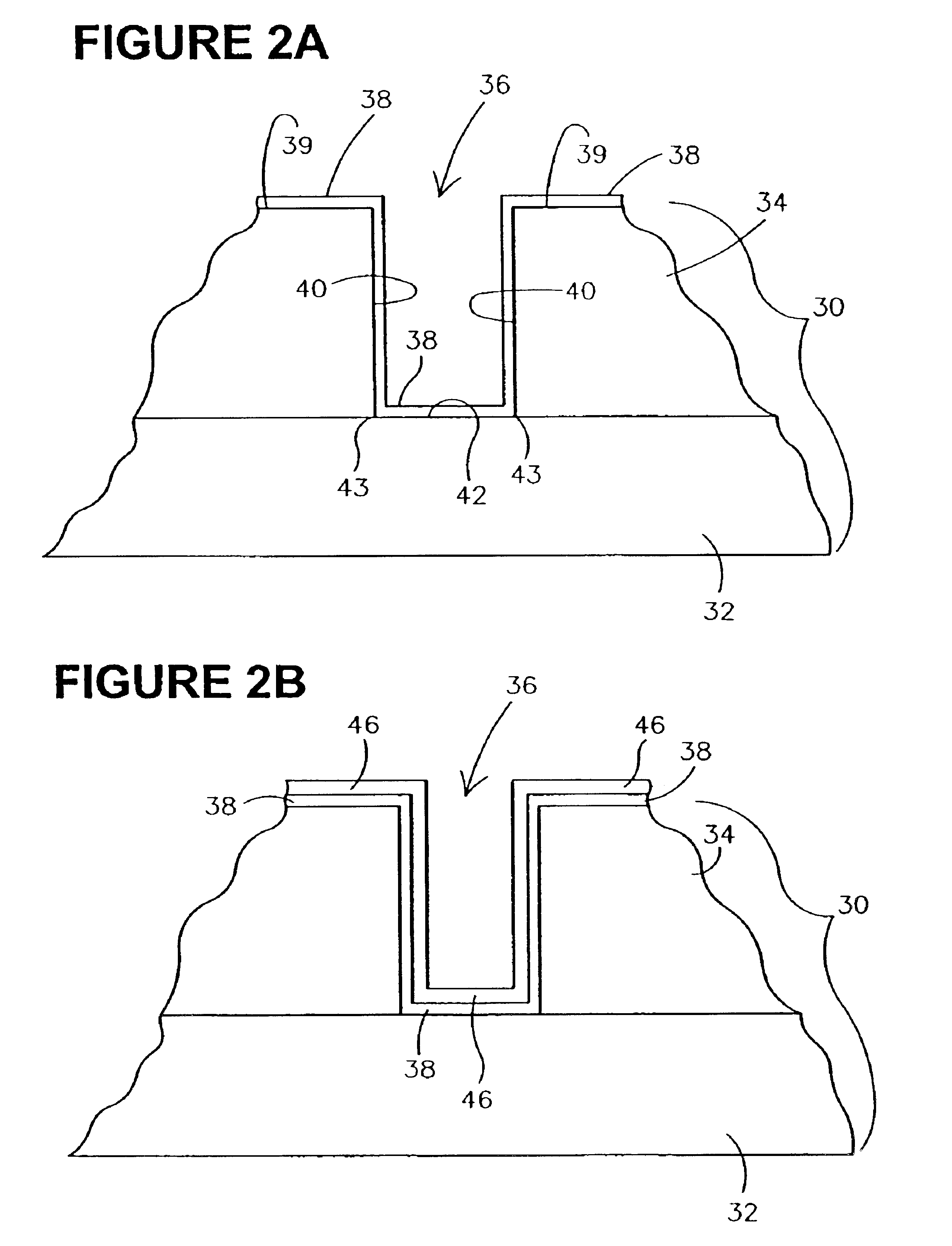
Methods for forming rough ruthenium-containing layers and structures/methods using same
a technology of ruthenium oxide and ruthenium oxide, which is applied in the direction of coatings, transistors, chemical vapor deposition coatings, etc., can solve the problems of reducing the reliability of the electrode connection, the use of hsg to enhance and the formation of silicon dioxide between the metal layer and the dielectric being formed, so as to increase the surface area of the lower electrode structure without increasing the occupation area of the capacitor structure, increase the surface area and reduce processing costs
- Summary
- Abstract
- Description
- Claims
- Application Information
AI Technical Summary
Benefits of technology
Problems solved by technology
Method used
Image

Examples
example 1
[0086]A rough ruthenium layer as shown in FIG. 4 was formed on an HF cleaned silicon wafer in a single wafer reaction chamber under the following conditions:[0087]a flow rate of about 200 sccm of helium carrier gas through a tricarbonyl (1,3-cyclohexadiene)Ru precursor held in a bubbler reservoir at room temperature (i.e.,about 25° C.);[0088]a deposition pressure of 3.0 torr; and[0089]a deposition temperature of 225° C.
example 2
[0090]A non-rough ruthenium layer as shown in FIG. 5 was formed on HF cleaned BPSG of a silicon wafer in a single wafer reaction chamber under the following conditions:[0091]a flow rate of about 200 sccm of helium carrier gas through a tricarbonyl (1,3-cyclohexadiene)Ru precursor held in a bubbler reservoir at room temperature (i.e. ,about 25° C.);[0092]a deposition pressure of 1.5 torr; and[0093]a deposition temperature of 250° C.
example 3
[0094]A ruthenium oxide layer that is not rough as shown in FIG. 6 was formed on an HF cleaned silicon wafer in a single wafer reaction chamber under the following conditions:[0095]a flow rate of about 225 sccm of helium carrier gas through a tricarbonyl (1,3-cyclohexadiene)Ru precursor held in a bubbler reservoir at room temperature (i.e.,about 25° C.);[0096]a flow rate of about 250 sccm of oxygen gas;[0097]a deposition pressure of 2.5 torr; and[0098]a deposition temperature of 210° C.
PUM
| Property | Measurement | Unit |
|---|---|---|
| temperature | aaaaa | aaaaa |
| pressure | aaaaa | aaaaa |
| temperature | aaaaa | aaaaa |
Abstract
Description
Claims
Application Information