Probing device and manufacturing method thereof, as well as testing apparatus and manufacturing method of semiconductor with use thereof

a technology of a probe device and a manufacturing method, which is applied in the direction of semiconductor/solid-state device testing/measurement, printed element electric connection formation, instruments, etc., can solve the problems of inability to achieve accurate inspection or test, limit the testing of high-speed signals, and cannot cope with the high density of electrodes. , to achieve the effect of high density, high accuracy and high density of objects

Inactive Publication Date: 2005-05-31
RENESAS ELECTRONICS CORP
View PDF47 Cites 119 Cited by
  • Summary
  • Abstract
  • Description
  • Claims
  • Application Information

AI Technical Summary

Benefits of technology

[0095]As is explained in the above, according to the above construction, a large number of the probes can be arranged with high density and high accuracy, as the result, it is possible to cope with high density of the object to be tested. Further, it is possible to shorten (from 0.001 to 0.2 mm) the length of the probes, as the result, it is possible to realize a high-speed AC testing with the stabilized high-speed signals, which can be supplied to all over the semiconductor elements with small voltage fluctuation. With this, confirmation of the high-speed operation as well as detailed observation of output wave-forms can be achieved, then margin of the semiconductor elements can be grasped, thereby enabling a feedback to the design of the semiconductor elements with high efficiency.

Problems solved by technology

However, with the testing method of the probe card which is shown as the prior art 1 in FIGS. 17 and 18 mentioned above, there is a limit for the testing with high speed signals due to the shape of the probe 5, in which lumped inductance is large.
Then the wave-form is rounded or deteriorated when dealing such the high speed signal, therefore it is impossible to achieve accurate inspection or test.
Further, with the probing method mentioned above, there is also a limitation in the special arrangement, therefore it cannot cope with the high density of the electrodes and the multiplication in the total number thereof on the semiconductor element.
However, it is difficult and not realistic to manufacture the such spring probe.
Moreover, with the prior art 3, since the projecting probe tip is ordinarily formed with the wet etching, the effect of so-called side etching is small, therefore it is difficult to manufacture it within a short time and with high efficiency.
Further, with this prior art 3, since the projecting probe tip is formed on the multi-layer print board, a softness thereof is lost, as the result, there is a risk that it gives injure onto the object to be tested, such as the semiconductor element, etc.

Method used


Image

  • Probing device and manufacturing method thereof, as well as testing apparatus and manufacturing method of semiconductor with use thereof
  • Probing device and manufacturing method thereof, as well as testing apparatus and manufacturing method of semiconductor with use thereof
  • Probing device and manufacturing method thereof, as well as testing apparatus and manufacturing method of semiconductor with use thereof

Examples


first embodiment

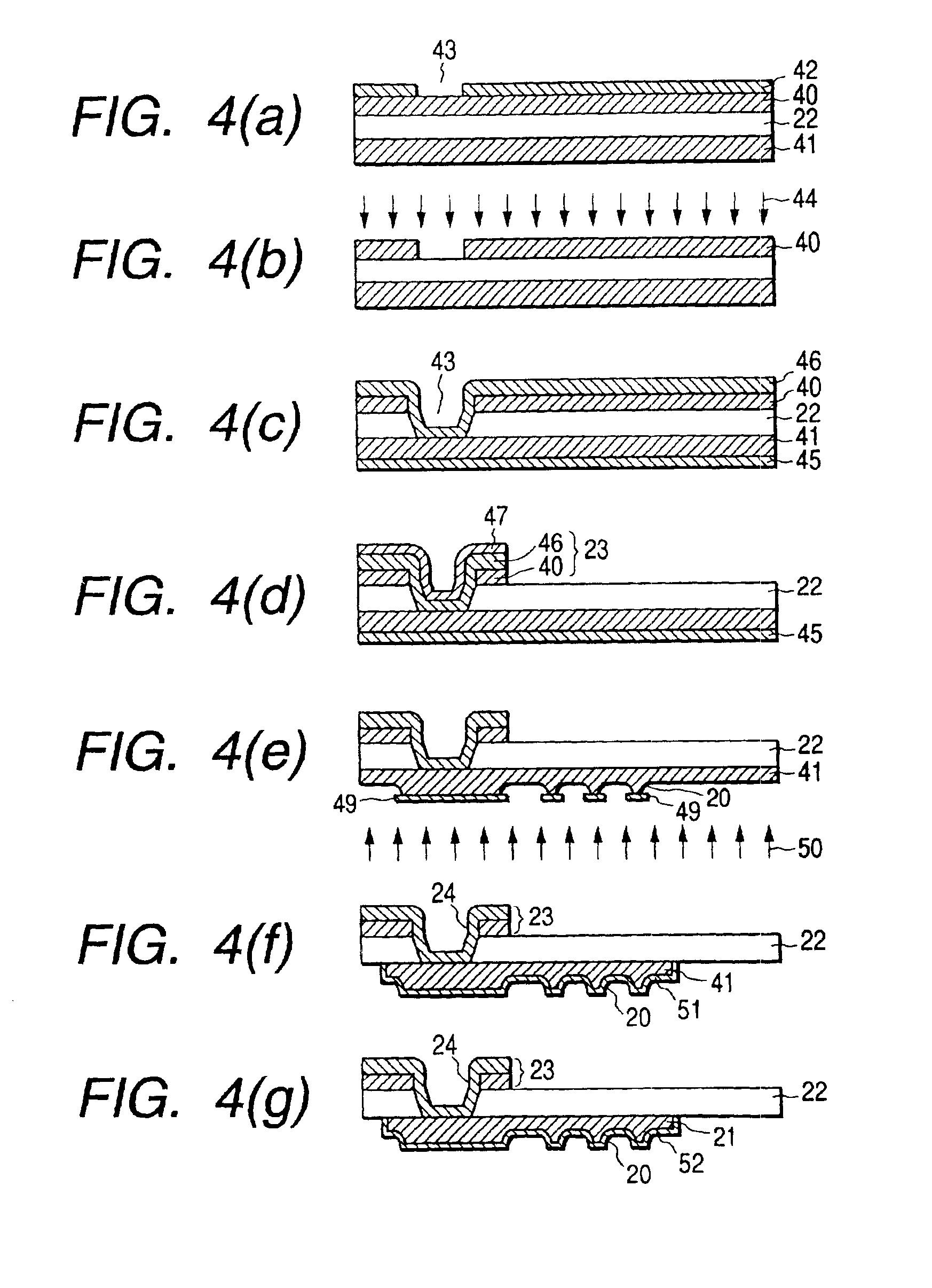
[0133]the wiring sheet constructing the probing device shown in FIG. 1 can be manufactured through the respective steps shown in FIGS. 4(a) through 4(g) mentioned in the above.

[0134]Next, a manufacturing process for forming the second embodiment of a wiring sheet, which constructs the probing device shown in FIG. 2, according to the present invention, will be explained by referring to FIG. 5. Namely, FIG. 5 shows a manufacturing process by the order of steps, in particular, for forming the tip portions 25 of the projection contact probes from a plating film, in the manufacturing process for forming the second embodiment of the wiring sheet constructing the probing device shown in FIG. 2.

[0135]First, a step shown in FIG. 5(a) is executed. In this step, in the same manner as in FIG. 4(a), the polyimide film 22 is prepared, on both surfaces of which are formed or covered with the thin copper films 40 and 41 of ordinary film thickness, i.e., approximately 18 μm or 25 μm. Photo-resist 42...

second embodiment

[0142]the wiring sheet constructing the probing device shown in FIG. 2 can be manufactured through the respective steps shown in FIGS. 5(a) through 5(g) mentioned in the above.

[0143]Next, a manufacturing process for forming the third embodiment of a wiring sheet, which constructs the probing device shown in FIG. 3, according to the present invention, will be explained by referring to FIG. 6. Namely, FIG. 6 shows a manufacturing process by the order of steps, in particular, for forming the tip portions 29 of the projection contact probes from a plating film, in the manufacturing process for forming the third embodiment of the wiring sheet constructing the probing device shown in FIG. 3.

[0144]Fist, as shown in FIG. 6, the same steps as shown in FIGS. 4(a) through 4(d) are executed. Those steps are for forming the electrode underground 30 by etching the copper thin film 41 with using the photo resist 57 after forming the extension wiring 33, being formed with the copper thin film 40 as...

third embodiment

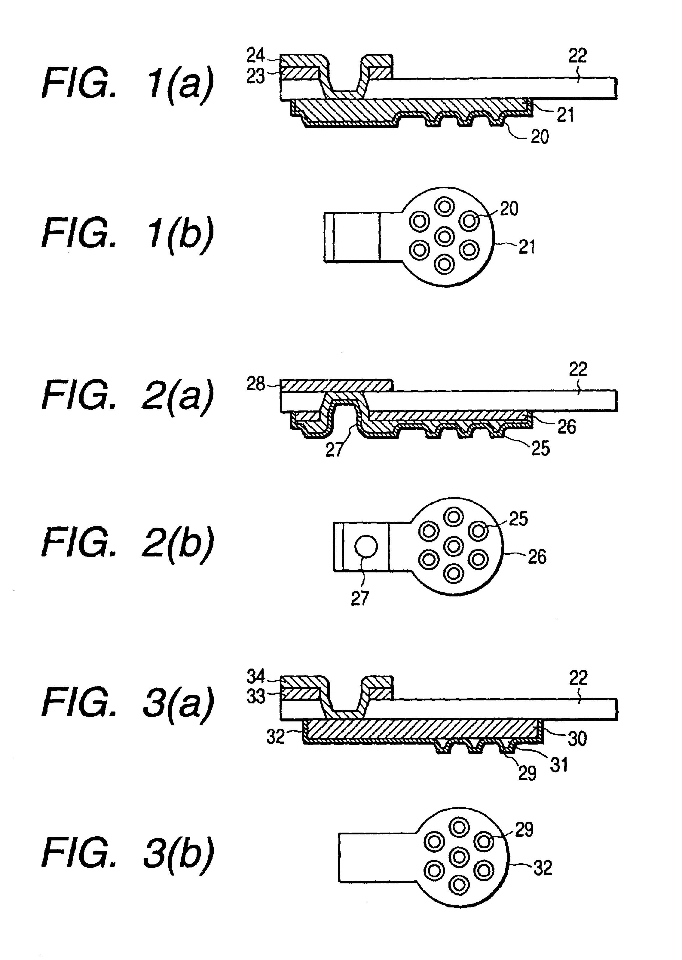
[0149]the wiring sheet constructing the probing device shown in FIG. 3 can be manufactured through the respective steps shown in FIGS. 4(a) through 4(d) and FIGS. 6(a) through 6(d) mentioned in the above. However, in this manufacturing process, since the plating material 31 such as the nickel or the like is formed on the copper thin film 30, the tip portions 29 of the one or more of contact probes can be produced easily with high accuracy, even if as the copper thin film 30 is applied the thin film having approximately 18 μm in the thickness, for example.

[0150]Next, a manufacturing process for forming an another embodiment of the wiring sheet constructing the probing device according to the present invention will be explained by referring to FIG. 7. FIG. 7 shows the manufacturing process for forming the tip portions of the projecting contact probes on a thin film of the another embodiment, in the order of steps thereof.

[0151]First, as shown in FIG. 7(a), the steps same to those show...


PUM


Abstract

A probing device for electrically contacting with a plurality of electrodes 3, 6 aligned on an object 1 to be tested so as to transfer electrical signal therewith, comprising: a wiring sheet being formed by aligning a plurality of contact electrodes 21, 110b, corresponding to each of said electrodes, each being planted with projecting probes 20, 110a covered with hard metal films on basis of a conductor thin film 41 formed on one surface of an insulator sheet 22 of a polyimide film by etching thereof, while extension wiring 23, 110c for electrically connecting to said each of said contact electrodes being formed on basis of a conductor thin film formed on either said one surface or the other surface opposing thereto of said insulator sheet of the polyimide film; and means for giving contacting pressure for obtaining electrical conduction between said extension wiring and said object to be tested by contacting tips of said projecting contact probe formed onto said each contact electrode through giving pressuring force between said wiring sheet and said object to be tested.

Description

[0001]This is a continuation application of U.S. Ser. No. 09 / 285,074, filed Apr. 2, 1999, now U.S. Pat. No. 6,617,863.BACKGROUND OF THE INVENTION[0002]1. Field of the Invention[0003]The present invention relates to a probing device and a manufacturing method thereof, as well as a testing apparatus and a manufacturing method with use thereof, in which electric signals are transferred through contact probes being contacted with electrodes opposing thereto on an object to be tested, and in particular to a probing device and a manufacturing method thereof, as well as a testing apparatus and a manufacturing method of a semiconductor with use thereof, especially being suitable for contacting with a large number of the electrodes provided on the semiconductor with high density.[0004]2. Description of Prior Art[0005]A wafer 1 shown in FIG. 16(A), on a surface of which are provided or constructed with a large number of semiconductor elements 2 (i.e., chips) for producing LSI, is cut and sepa...

Claims


Application Information

Patent Timeline
Patent Type & Authority Patents(United States)
IPC IPC(8): G01R1/067G01R1/073H05K3/40G01R3/00G01R31/26G01R31/28H01L21/66
CPCH05K3/4007G01R1/0735G01R1/06738G01R3/00
Inventor KASUKABE, SUSUMUHASEBE, AKIO
Owner RENESAS ELECTRONICS CORP
Why Eureka
Try Eureka