Systems and methods for epitaxially depositing films on a semiconductor substrate

a technology of epitaxial depositing and semiconductor substrates, applied in the direction of chemically reactive gases, coatings, crystal growth processes, etc., can solve the problems of increasing the difficulty of maintaining the necessary level of control, increasing the difficulty of conventional epitaxial depositing approaches reducing the difficulty and risk of lifting pin breakage, and reducing the amount of time required

Inactive Publication Date: 2005-06-07
MATTSON TECHNOLOGY +1
View PDF66 Cites 37 Cited by
  • Summary
  • Abstract
  • Description
  • Claims
  • Application Information

AI Technical Summary

Benefits of technology

[0019]In another embodiment of the present invention, the lift pin mechanism that raises a substrate off a susceptor is capable of rotating with the susceptor during processing. This ability to rotate the lift pins with the susceptor eliminates the difficulty and risk of lift pin breakage associated with stopping the r...

Problems solved by technology

Maintaining the required level of control, however, has proven increasingly difficult to achieve due to the recent transition from 200 mm to 300 mm fabrication processes, the tighter process specifications imposed by many semiconductor manufacturers and the higher throughput requirements (the number of substrates processed per unit of time) necessary for cost-effective manufacturing.
In light of these increased processing demands, maintaining the necessary level of control while simultaneously satisfying throughput requirements, has proven increasingly difficult to achieve using conventional epitaxial deposition approaches.
If the surface energy is insufficient for a reactant to become accommodated at a lattice site before additional atoms have accumulated over it, undesirable defects in the crystal lattice will occur.
Conventional epitaxial reactors, such as the reactor illustrated in FIG. 1, suffer from several deficiencies which may prevent these reactors from providing an effective and cost-efficient solution for various applications.
One problem is that the bell-shaped jar 101 has a relatively large volume which inhibits the ability of the reactor to precisely control the processing temperature of the semiconductor substrate 102 and the process gases.
If the temperature is too low, the reactants will h...

Method used


Image

  • Systems and methods for epitaxially depositing films on a semiconductor substrate
  • Systems and methods for epitaxially depositing films on a semiconductor substrate
  • Systems and methods for epitaxially depositing films on a semiconductor substrate

Examples


Embodiment Construction

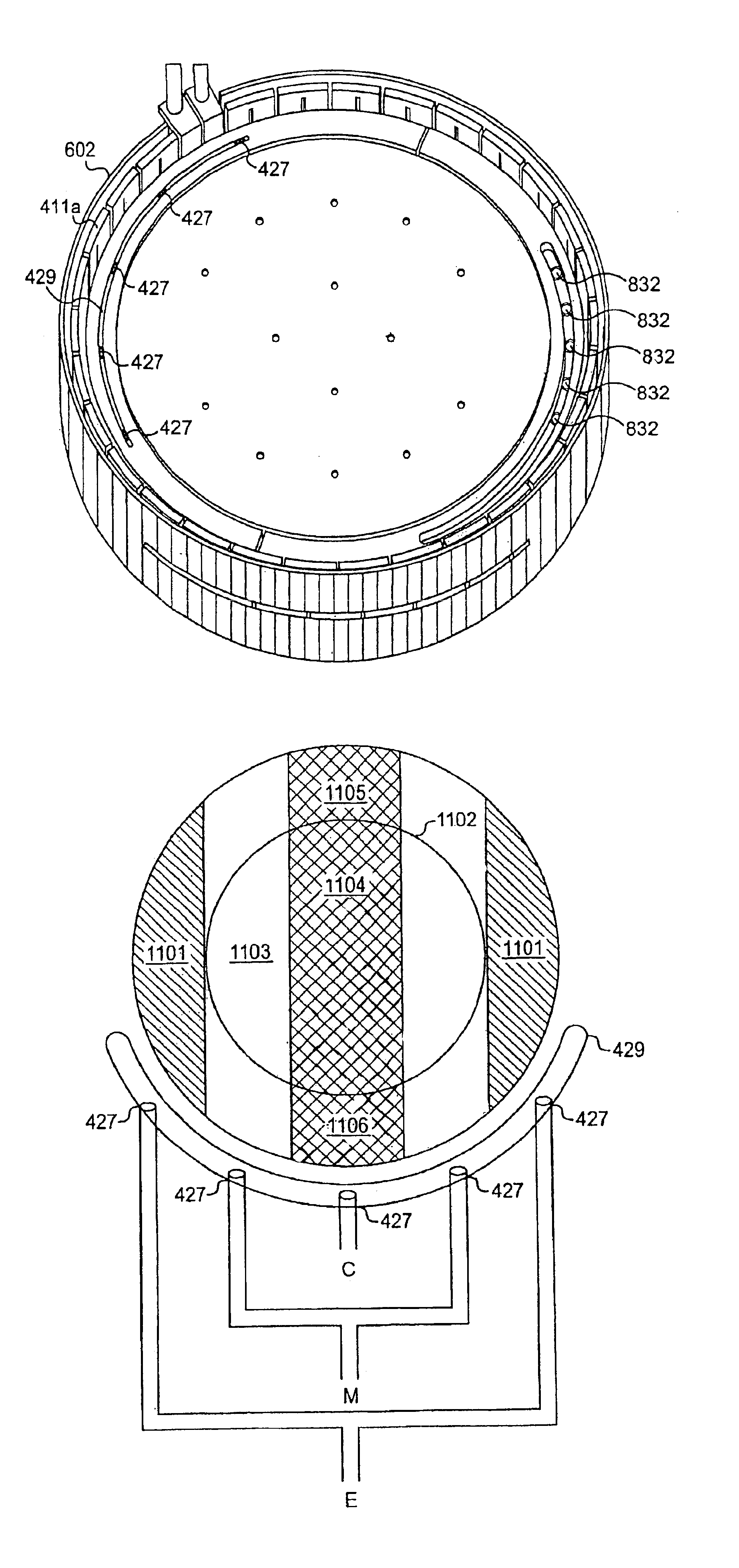
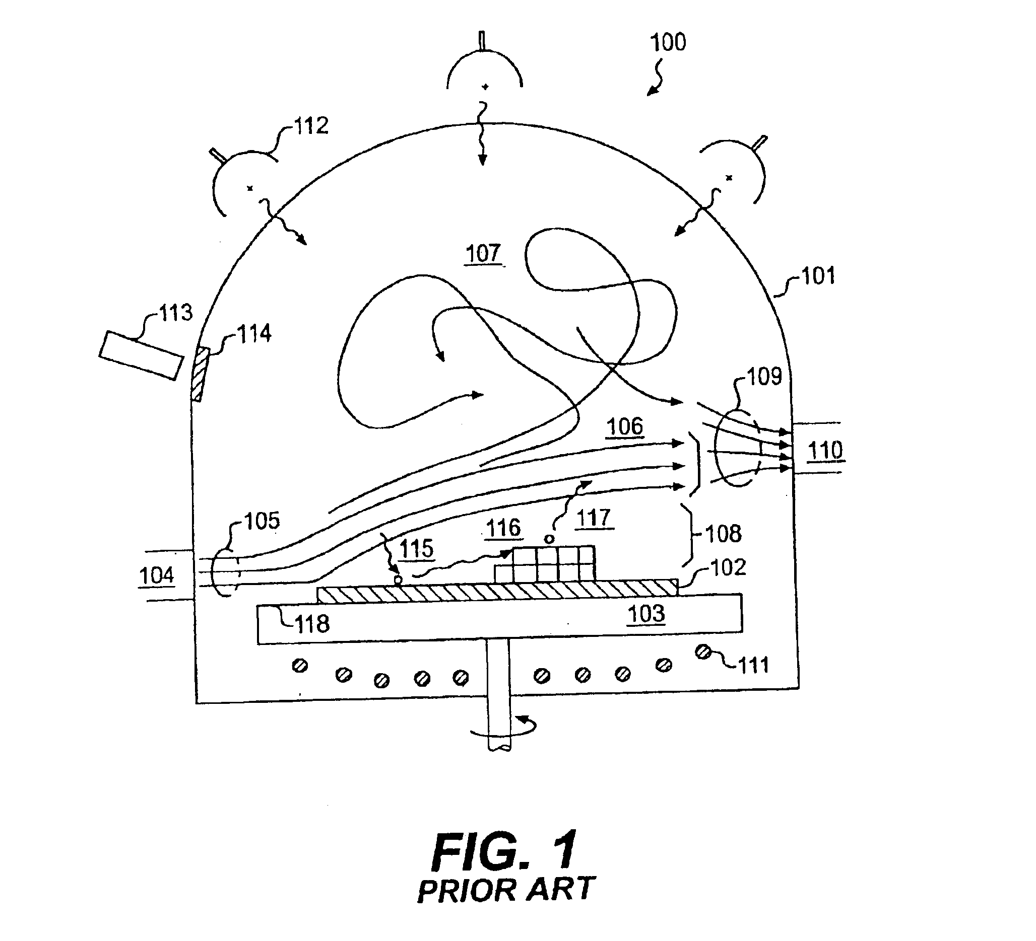
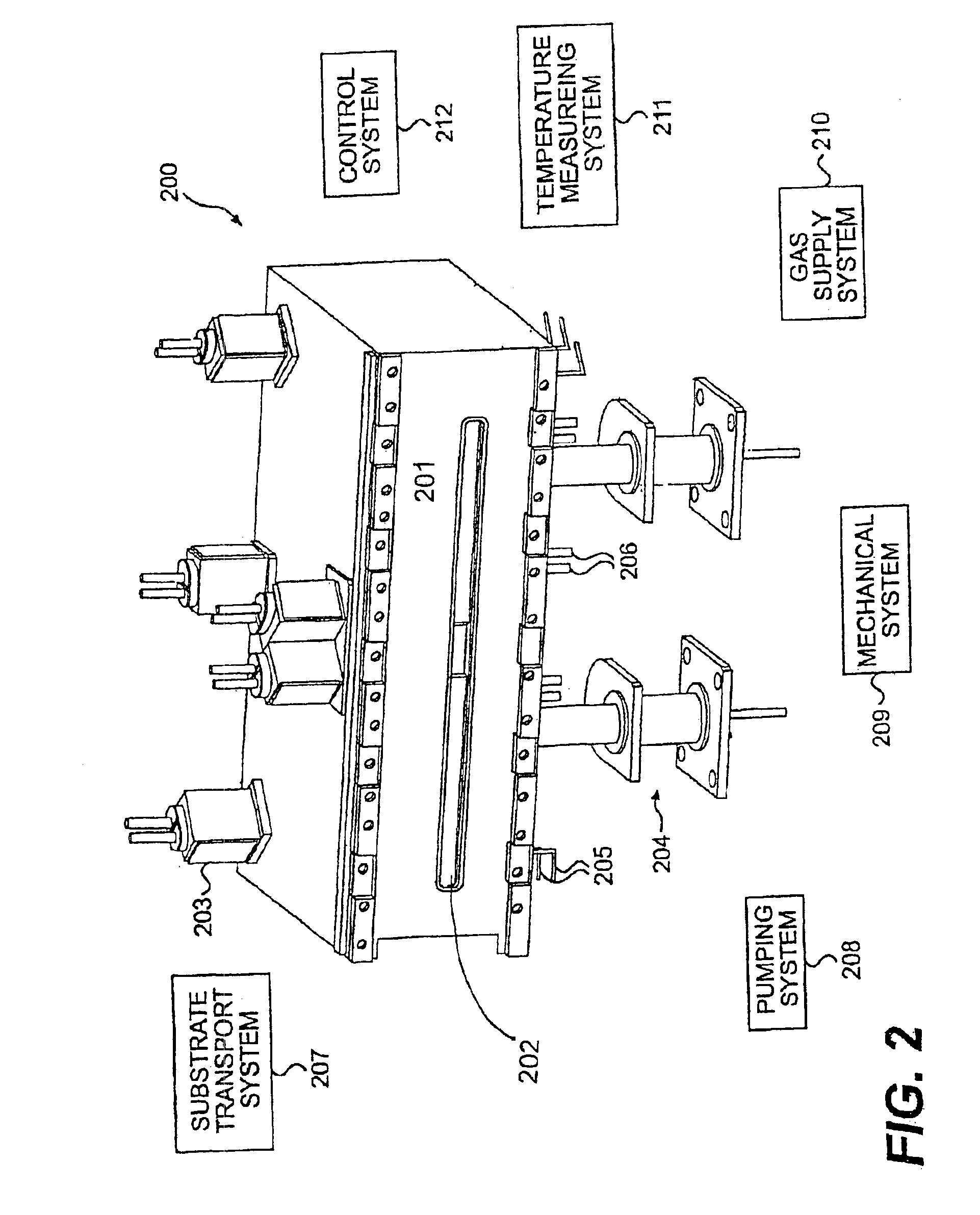
[0040]Aspects of the present invention provide improved systems and methods for processing semiconductor substrates. An exemplary embodiment of the present invention provides a stable, hot-walled thermal environment for epitaxial or potentially any other thermal CVD deposition on semiconductor wafers. An insulated processing cavity is formed from opaque quartz walls and a rotating susceptor and may enclose or be surrounded by a resistive heating system. The walls thermally insulate the processing cavity from the cooler surrounding environment and provide a relatively uniform and stable thermal processing environment. The processing environment may also be maintained at vacuum pressure to increase insulation and the stability of the thermal environment. Wafers are inserted through a narrow slot into the processing environment and onto pins which lower the wafer on the heated susceptor. The wafer is rotated on a susceptor and a silicon deposing gas is flowed across the surface of the ...


PUM

PropertyMeasurementUnit
Temperatureaaaaaaaaaa
Flow rateaaaaaaaaaa
Concentrationaaaaaaaaaa

Abstract

Systems and methods for epitaxial deposition. The reactor includes a hot wall process cavity enclosed by a heater system, a thermal insulation system, and chamber walls. The walls of the process cavity may comprises a material having a substantially similar coefficient thermal expansion as the semiconductor substrate, such as quartz and silicon carbide, and may include an isothermal or near isothermal cavity that may be heated to temperatures as high as 1200 degrees C. Process gases may be injected through a plurality of ports, and are capable of achieving a fine level of distribution control of the gas components, including the film source gas, dopant source gas, and carrier gas. The gas supply system includes additional methods of delivering gas to the process cavity, such as through temperature measurement devices, and through a showerhead.

Description

RELATED APPLICATIONS[0001]The present application is based on and claims priority to a provisional application filed on Apr. 12, 2001, having U.S. Ser. No. 60 / 283,541.BACKGROUND OF THE INVENTION[0002]The present invention relates in general to the processing of semiconductor substrates, and more particularly, to improved systems and methods for epitaxially depositing films onto a semiconductor substrate.[0003]Processes utilizing epitaxial deposition generally involve the growth of one or more layers or films onto a semiconductor substrate. The growth of these layers is carefully controlled by the underlying processes and equipment to produce layers having the desired physical, electrical and mechanical characteristics. These characteristics typically include, for example, the growth rate and thickness of the epitaxial layer, resistivity, dopant concentration, doping transition width, defect density, level of metal and particle contamination, and slip. Because these characteristics a...

Claims


Application Information

Patent Timeline
IPC IPC(8): C23C16/458C30B25/08C23C16/46C30B25/14C23C16/455H01L21/00H01L21/687H01L21/67C23C16/44H01L21/205
CPCC23C16/455C23C16/45504C23C16/45519C23C16/45578C23C16/4584C23C16/46H01L21/68785C30B25/14H01L21/67017H01L21/6715H01L21/68742H01L21/68771C30B25/08H01L21/20
Inventor JOHNSGARD, KRISTIAN E.SALLOWS, DAVID E.MESSINEO, DANIEL L.MAILHO, ROBERT D.JOHNSGARD, MARK W.
Owner MATTSON TECHNOLOGY
Why Eureka
Try Eureka