Semiconductor device and manufacturing method thereof

Inactive Publication Date: 2005-06-14
SEMICON ENERGY LAB CO LTD
View PDF65 Cites 47 Cited by
  • Summary
  • Abstract
  • Description
  • Claims
  • Application Information

AI Technical Summary

Benefits of technology

[0011]The present invention carries out a further improvement of a pixel section, based on the structure described in the above publications. S

Problems solved by technology

However, it is difficult to satisfy all of the circuit specifications with TFTs having the same structure

Method used


Image

  • Semiconductor device and manufacturing method thereof
  • Semiconductor device and manufacturing method thereof
  • Semiconductor device and manufacturing method thereof

Examples


embodiment 1

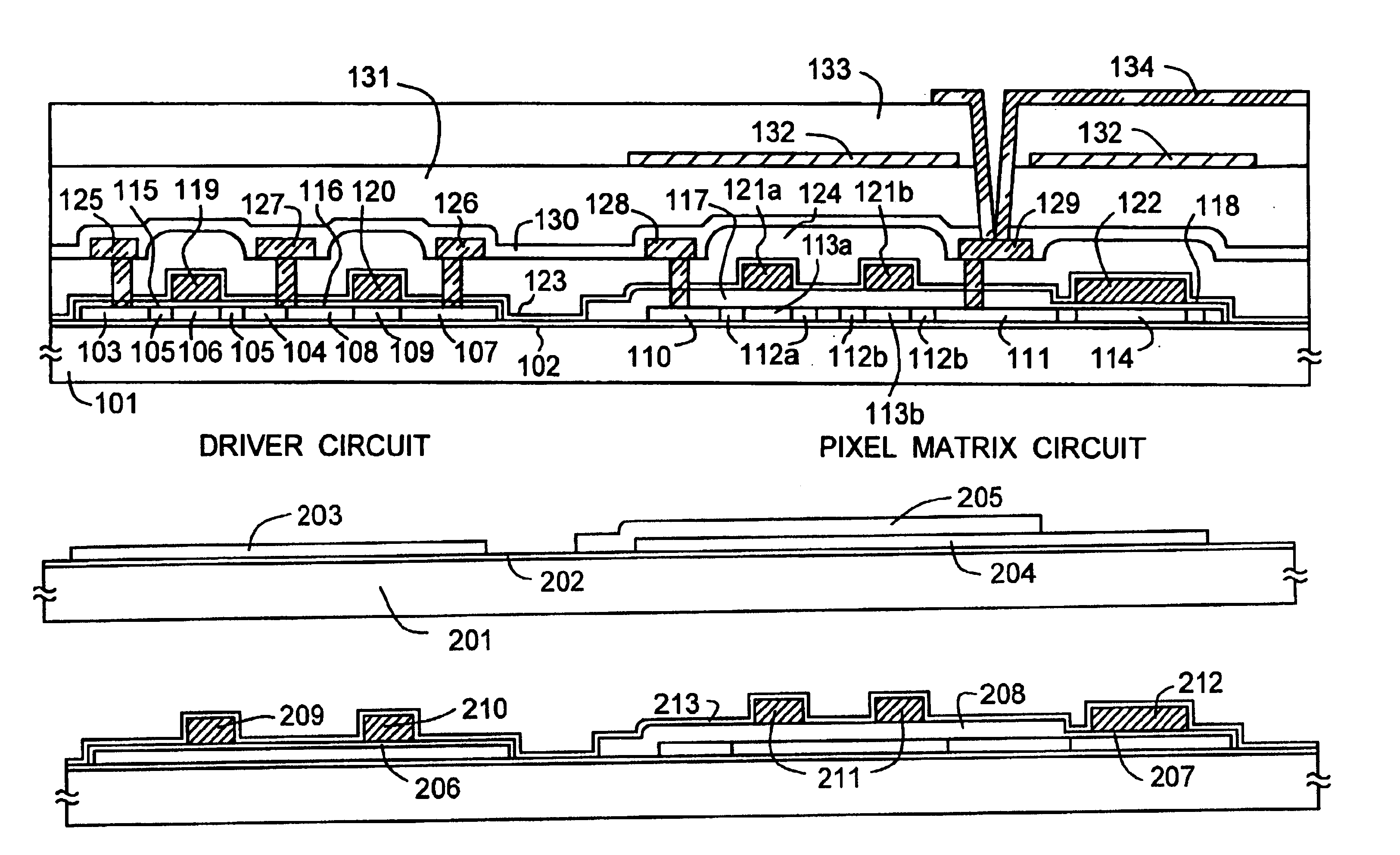
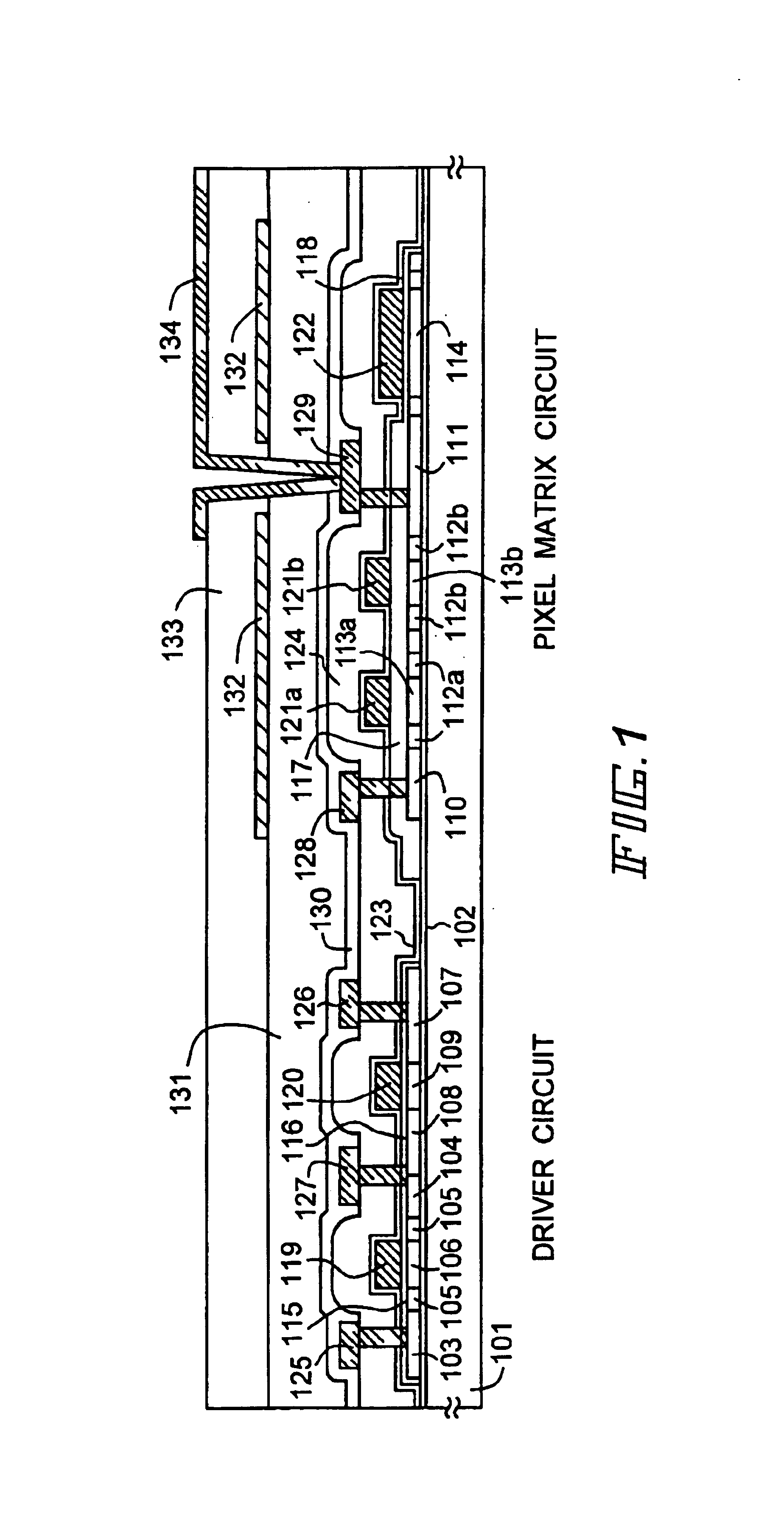
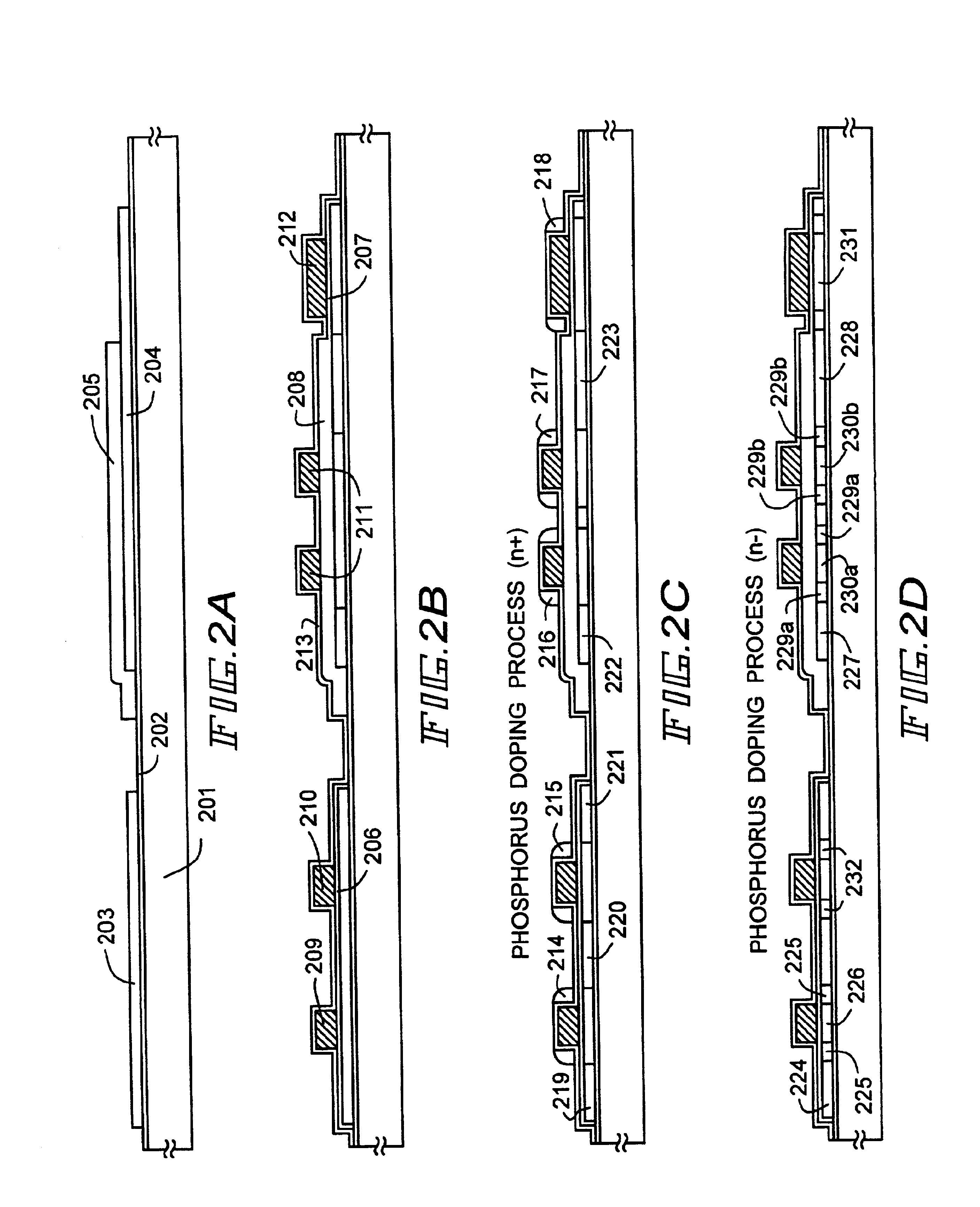
[0127]The method of manufacture to realize the structure in FIG. 1, which is explained in the detailed description of the preferred embodiments of the present invention, is explained in embodiment 1. FIGS. 2A to 3C are used in the explanation.

[0128]First, a quartz substrate 201 is prepared as a substrate, and a 20 nm silicon oxide film 202 and an amorphous silicon film (not shown) are formed successively on top, without being released to the atmosphere. By doing so, impurities included in the atmosphere, such as boron, can be prevented from being absorbed with the lower surface of the amorphous silicon film.

[0129]Note that an amorphous silicon film is used in embodiment 1, but other semiconductor films may also be used. A microcrystalline silicon film is acceptable, as is an amorphous silicon germanium film.

[0130]Crystallization of the amorphous silicon film is performed next. The technique described in Japanese Patent Application Laid-Open No. Hei 9-312260 is used as the crystalliz...

embodiment 2

[0202]FIGS. 4A to 4D are used in embodiment 2 to specifically explain what type of TFT structures are placed in what kind of circuits.

[0203]The minimum required operation voltage (power supply voltage) differs for an AM-LCD depending upon the circuit. For example, considering the voltage applied to the liquid crystals and the voltage for driving pixel TFTs in the pixel section, the operation voltage becomes from 14 to 20 V. Therefore, a TFT which can withstand the application of that much high voltage must be used.

[0204]In addition, a shift register circuit, etc., used in a source driver circuit or in a gate driver circuit operates sufficiently at approximately 5 to 10 V. There are advantages of more compatibility with an external signal, and lower power consumption, the lower the operation voltage. However, operation speed is sacrificed as a substitute for good voltage resistance characteristics in the high voltage resistant type TFT stated above, and therefore it is not suitable f...

embodiment 3

[0217]During the selective removal process of the gate insulating film 205 in embodiment 1, it is desirable to perform removal in the regions which become driver TFTs and storage capacitors as shown in FIG. 5. In FIG. 5 reference numeral 501 denotes an active layer, 502 denotes an end section of the gate insulating film 205, and 503 and 504 denote gate wirings. It is desirable to leave the gate insulating film 205 in the end portion of the active layer 501, in areas 505 where the gate wirings overlap the active layer, as shown in FIG. 5.

[0218]A phenomenon called edge thinning occurs in the end portion of the active layer 501 when a later thermal oxidation process is performed. This is a phenomenon in which the oxidation reaction proceeds so as to dig under the end portion of the active layer, with the end portion getting thinner and at the same time rising up. Therefore, if the edge thinning phenomenon occurs, then a problem develops where the gate wiring is easily cut when the gate...


PUM


Abstract

A semiconductor device having high reliability, in which TFTs with appropriate structures for the circuit functions are arranged, is provided. Gate insulating films (115) and (116) of a driver TFT are designed thinner than a gate insulating film (117) of a pixel TFT in a semiconductor device having a driver circuit and a pixel section on the same substrate. In addition, the gate insulating films (115) and (116) of the driver TFT and a dielectric (118) of a storage capacitor are formed at the same time, so that the dielectric (118) may be extremely thin, and a large capacity can be secured.

Description

[0001]This application is a divisional of U.S. application Ser. No. 09 / 477,865, filed on Jan. 5, 2000 now U.S. Pat. No, 6,278,131.BACKGROUND OF THE INVENTION[0002]1. Field of the Invention[0003]The present invention relates to a semiconductor device having a circuit comprising thin film transistor (hereinafter referred to as TFT). For example, it relates to structures of an electro-optical device which is typified of a liquid crystal display device or an EL display device and electric equipment which uses a semiconductor circuit and an electro-optical device or a semiconductor circuit of the present invention.[0004]Note that through this specification, a semiconductor device indicates devices in general which may function by making use of semiconductor characteristics, and that electro-optical devices, semiconductor circuits, and electric equipments are all semiconductor devices.[0005]2. Description of the Related Art[0006]A thin film transistor (hereinafter referred to as TFT) can ...

Claims


Application Information

Patent Timeline
IPC IPC(8): H01L21/70H01L21/84H01L27/12G02F1/13G02F1/1362H01L21/77H01L27/13H01L29/04H01L29/423H01L29/786
CPCH01L27/1237H01L27/1277H01L27/1255H01L29/42384G02F1/13454H01L29/78645
Inventor YAMAZAKI, SHUNPEIKOYAMA, JUNSHIBATA, HIROSHIFUKUNAGA, TAKESHI
Owner SEMICON ENERGY LAB CO LTD
Why Eureka
Try Eureka