Ceramic electronic component
a technology of ceramic electronic components and ceramics, applied in the direction of resistive material coating, positive temperature coefficient thermistors, titanium compounds, etc., can solve the problems of deterioration of the protective layer of the ceramic electronic component formed by coating an organic resin or an inorganic glass, the component has to be burned in the reducing atmosphere, and the protective layer cannot be used for a long time. , to achieve the effect of reducing the withstand voltage of the ceramic, reducing the p
- Summary
- Abstract
- Description
- Claims
- Application Information
AI Technical Summary
Benefits of technology
Problems solved by technology
Method used
Image
Examples
example 1
[0021]BaCO3, TiO2 and Sm2O3 were blended to prepare the following powder for semiconductive ceramic composition:
(Ba0.998 Sm0.002)1.002 TiO3
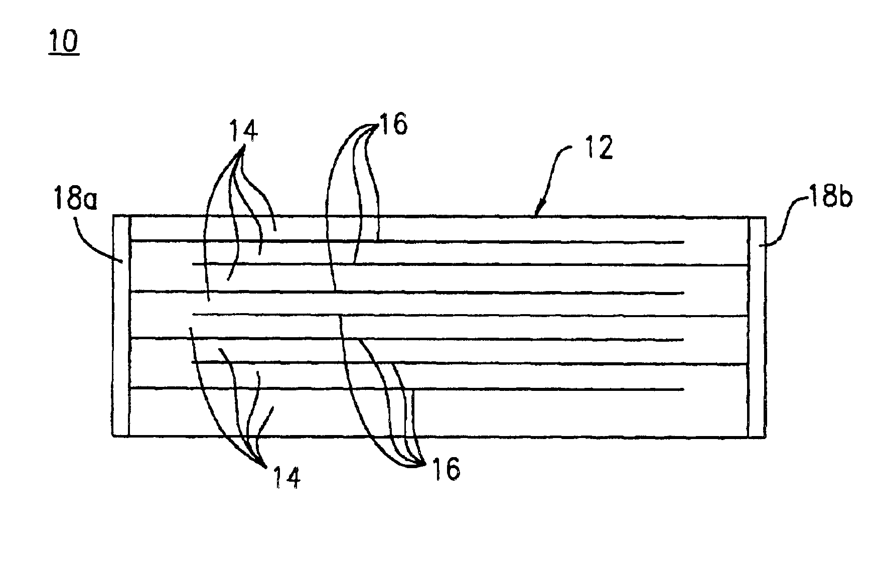
The powder was pulverized with zirconia balls in water for 5 hours and calcined at 1100° C. for 2 hours. After an organic binder was added, the mixture was formed into sheets. Then, Ni internal electrodes were printed thereon. The sheets were stacked and subsequently burned at 1200° C. in a reducing atmosphere of H2 / N2. Next, the sheets were provided with external electrodes formed of Ag and reoxidized at 700° C. in air to prepare the PTC thermistor shown in FIG. 1.
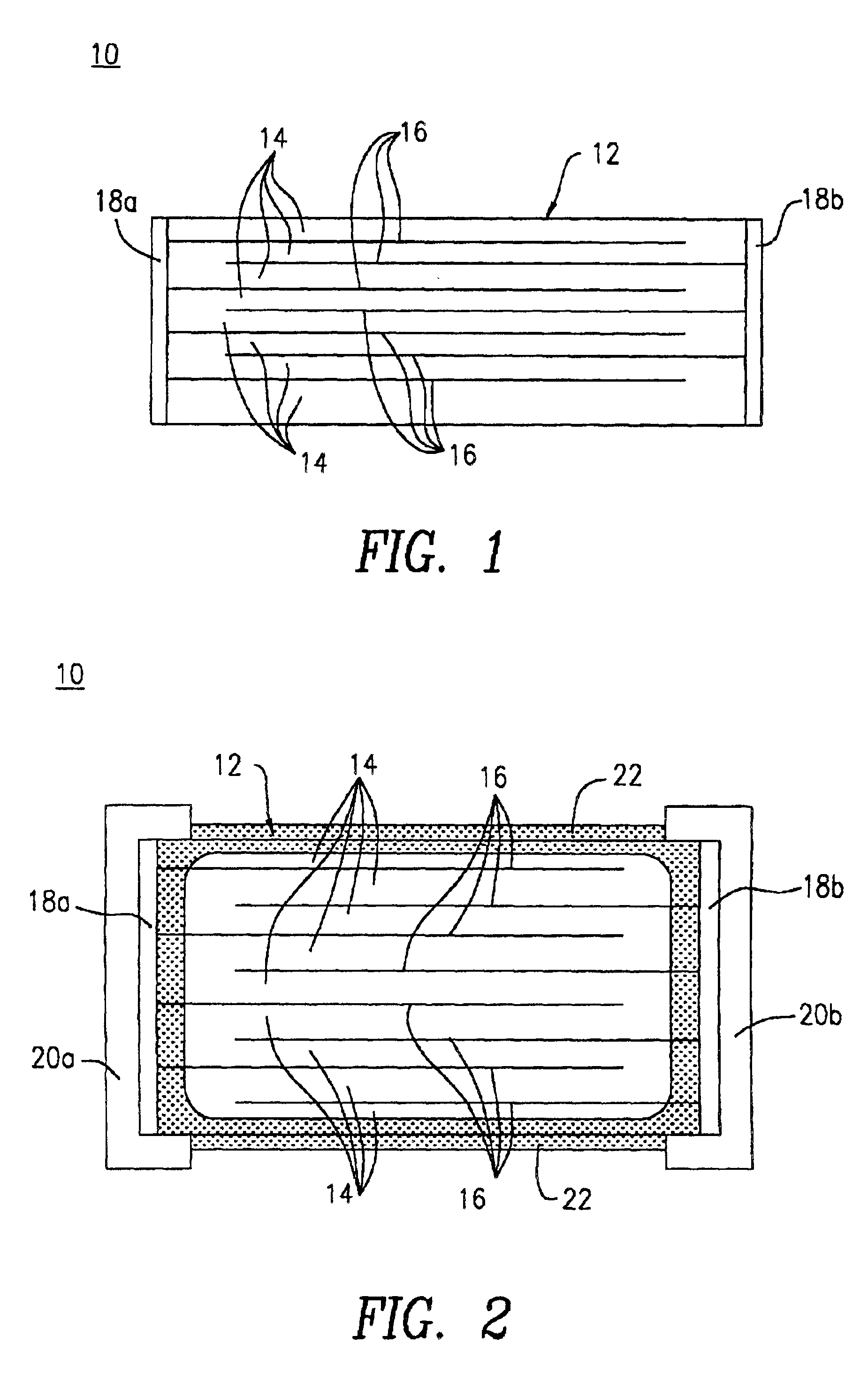
[0022]The PTC thermistor 10 shown in FIG. 1 comprises a component body 12. The component body 12 comprises a plurality of semiconductive ceramic layers 14 and a plurality of internal electrodes 16. The semiconductive ceramic layers 14 and the internal electrodes 16 are alternately laminated. The internal electrodes 16 are alternately exposed at one side of the component body 12 and the...
example 2
[0024]A PTC thermistor 10 was prepared in the same process as Example 1 except for replacing the glass solution with a Li—Si—O glass solution, and then the resistance at room temperature and the withstand voltage were measured.
example 3
[0025]A PTC thermistor 10 was prepared in the same process as Example 1 except for replacing the glass solution with a K—Si—O glass solution, and then the resistance at room temperature and the withstand voltage were measured.
PUM
| Property | Measurement | Unit |
|---|---|---|
| softening point | aaaaa | aaaaa |
| withstand voltage | aaaaa | aaaaa |
| molar ratio | aaaaa | aaaaa |
Abstract
Description
Claims
Application Information

