
Method for forming a semiconductor device

a semiconductor and device technology, applied in the field of partial doping technology, can solve the problems of difficulty in forming a shallow impurity layer, reducing yield, redistribution and defect of impurities, etc., and achieve the effect of reducing the resistance rate of said region

Inactive Publication Date: 2005-07-19
SEMICON ENERGY LAB CO LTD
View PDF36 Cites 3 Cited by
  • Summary
  • Abstract
  • Description
  • Claims
  • Application Information

AI Technical Summary

Benefits of technology

The present invention provides a method for improving doping efficiency in semiconductor devices using a laser beam. The invention proposes methods for selectively doping semiconductor regions with different impurities using a mask and a laser beam. The invention also allows for the simultaneous doping of multiple impurities and the simultaneous polycrystallization of an amorphous semiconductor. The invention utilizes the phenomenon of impurity diffusion into semiconductor regions and allows for selective doping without the need for photolithography. The technical effects of the invention include improved doping efficiency, simplified device preparation, and improved device performance.

Problems solved by technology

(1) In case where an impurity is doped in a semiconductor by a heat-diffusion method, there poses a problem that a high temperature process is required. For example of a silicon semiconductor, it is necessary to heat a silicon semiconductor sample at a temperature of 1000 to 1200° C., thereby making it difficult to form a shallow impurity layer which is required for a high density IC, and posing a problem of impurity redistribution and defect resulted from the high temperature process.
(2) In case of the impurity doping method by an ion-implantation, there poses the same problem as mentioned in the above (1), because it is in need of a post heat-treatment at a temperature of 600 to 950° C., to activate the impurity and to recover the defect.
Also, as a problem in common with the heat-diffusion method and the ion-implantation method stated above, both of them need a high temperature process extremely over 600° C. For example, in case of an active matrix type liquid crystal display device to which an attention has been paid recently, since MOS type thin film transistor (TFT) is formed on a glass substrate, it has been difficult to employ the above heat-diffusion method and the ion-implantation method, if a cheap glass substrate which has a heat resistant temperature of 600 to 700° C. is used.
Then, a photolithography process followed by a complicated process will be required, and it has been well known that the photolithography causes a yield to be lowered.
As noted above, there has been a preparing problem that the high temperature process is required in the conventional impurity doping method, and further, a mask forming process, which is in need of a photolithography process for the selective doping, is required.
Also, the structure of TFT takes an inverse stagger type, and as a structural problem, it has been prone to generate a parasitic capacity.
These methods, however, have been in need of the post heat-treatment process at a temperature of 600 to 950° C., so as to activate an impurity and recover a defect, as mentioned above, and it has been industrially difficult to use them, considering that a heat resistant temperature of a cheap glass substrate is in the range of 600 to 700° C.
But it poses a problem that a doping efficiency will be lowered, as an energy will not be absorbed in a reactive gas according to the wave length of laser beam.
So that, in case where the doping of different element has to be effected, by using various kind of reaction gases, there arises a problem that the doping concentration will be disproportioned.
Therefore, this has been a problem that the doping gas is restricted owing to a sort of laser, and the laser suitable for each doping gas should be respectively prepared.

Method used


Image

  • Method for forming a semiconductor device
  • Method for forming a semiconductor device
  • Method for forming a semiconductor device

Examples


example 1

[0048]The present Example deals with a selective doping executed in a preparing process for a N-channel type MOSFET of silicon gate, using a mask by a laser beam according to the present invention. In all the Examples described hereinafter, a well known semiconductor device employing a silicon semiconductor was used.

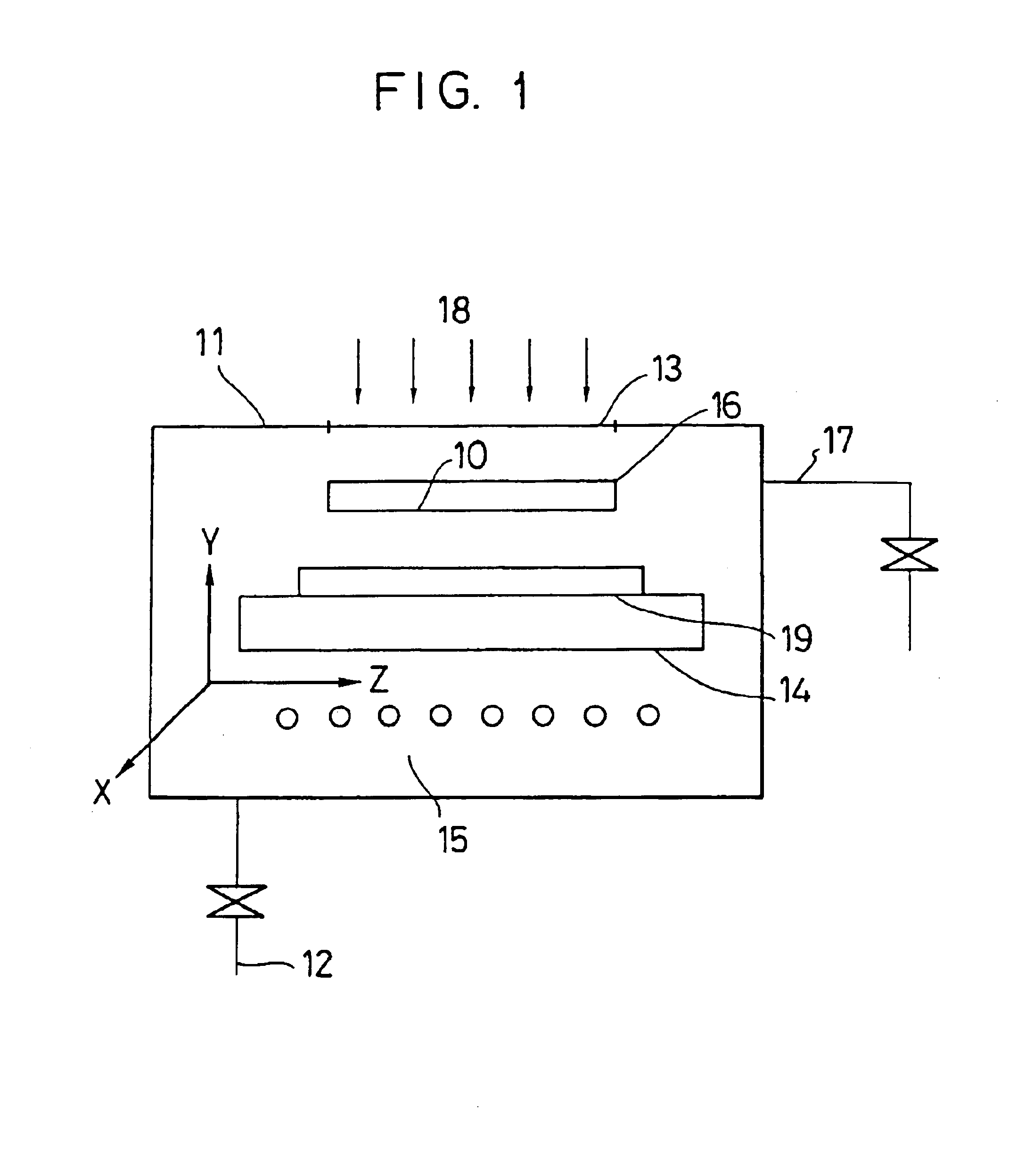
[0049]Firstly, a laser doping system used in the present Example is indicated in FIG. 1, in which the numeral 11 indicates a vacuum chamber equipped with a high vacuum exhausting system 12. The high vacuum exhausting system 12 is connected in series to a rotary pump and a turbo-molecule pump, and operates so as to prevent a disused impurity from being remained in the vacuum chamber 11 to the utmost, by once exhausting air up to a high vacuum state, when an atmosphere in the vacuum chamber 11 is changed over. The numeral 17 indicates an introducing system of a reactive gas and a diluted gas, through which such reactive gas containing one conductivity element as PH3 or B2H...

example 2

[0061]The present Example deals with the application of the present invention in a preparing process of C / TFT which is formed as a complementary, using N-channel type MOSTFT (hereinafter refer to as NTFT) and P-channel type MOSTFT (hereinafter refer to as PTFT) provided on a glass substrate. In this Example, a silicon semiconductor was also used as a semiconductor. Of course, it is needless to say that the impurity doping technology, which will be explained in this Example, can be applied to the preparation of CMOS integrated circuit on a silicon substrate.

[0062]The preparing process of the present Example is shown in FIG. 3, and the completed upper view of the present Example, which represent CMOS device provided on a glass substrate as a complementary using PTFT and NTFT (hereinafter referred to as C / TFT), is shown in FIG. 3(A). In FIG. 3, the numerals 39 and 392 indicate an input wiring of C / TFT, 393 indicates an output wiring, and 391 indicates a gate electrode wiring. The numer...

example 3

[0076]The present Example deals with the case, wherein the doping method according to the present invention is applied to a preparation for N-channel thin film type insulating gate field effect transistor (hereinafter referred to as NTFT) provided on a glass substrate.

[0077]In this Example, a glass substrate or a quartz substrate was used as a substrate. This was resulted from the intention that TFT prepared in this Example was used, in an active matrix type liquid display device or a switching element and a driving element of an image sensor. Of course, the present invention can be applied to a doping technology in the formation of P-type semiconductor layer and N-type semiconductor layer in the photo-electric conversion device, and further in the preparation of integrated circuit. Therefore, as a substrate, a silicon or a substrate of single crystal, or polycrystal of other semiconductor, and other insulator can be used.

[0078]Firstly, in FIG. 5, SiO2 film or silicon nitride film w...


PUM


Abstract

A method for forming a semiconductor device is disclosed. The method comprises the step of irradiating a laser light to a surface of a semiconductor through a mask provided on said surface in an atmosphere comprising an impurity of one conductivity type to diffuse said impurity into a region of said semiconductor.

Description

[0001]This application is a Div of Ser. No. 09 / 222,776 Dec. 30, 1998 U.S. Pat. No. 6,660,575 which is a Div of Ser. No. 08 / 300,938 Sep. 6, 1994 U.S. Pat. No. 5,938,839 which is a CON of Ser. No. 07 / 956,860 Oct. 5, 1992 ABN.BACKGROUND OF THE INVENTION[0002]1. Field of the Invention[0003]The present invention relates to a partial doping technology with an impurity, which is necessary for a preparing process of such semiconductor device as MOS (Metal-Oxide-Semiconductor) type or CMOS (Complementary Metal-Oxide-Semiconductor) type semiconductor device. In particular, the present invention provides a doping technology, which is capable of a selective method to dope a different region with a different impurity, using a simple and convenient process, and also which is capable of an efficient doping in a low temperature process.[0004]2. Description of the Related Art[0005]It is indispensable to arrange a process for partially controlling of a resistance rate, by adding an impurity which sel...

Claims


Application Information

Patent Timeline
Patent Type & Authority Patents(United States)
IPC IPC(8): H01L21/336H01L21/223H01L21/02H01L21/70H01L21/84H01L21/22H01L21/77
CPCH01L21/223H01L21/84H01L27/1214H01L29/66757Y10S117/904H01L27/1274H01L27/127H01L21/268
Inventor ZHANG, HONGYONG
Owner SEMICON ENERGY LAB CO LTD
Learn More