

Determination of minority carrier diffusion length in solid state materials
a technology of diffusion length and minority carrier, applied in the direction of contactless testing, individual semiconductor device testing, instruments, etc., to achieve the effect of fast mapping of diffusion length and significant reduction of measurement tim
- Summary
- Abstract
- Description
- Claims
- Application Information
AI Technical Summary
Benefits of technology
Problems solved by technology
Method used
Image

Examples
Embodiment Construction
Probe and Apparatus:
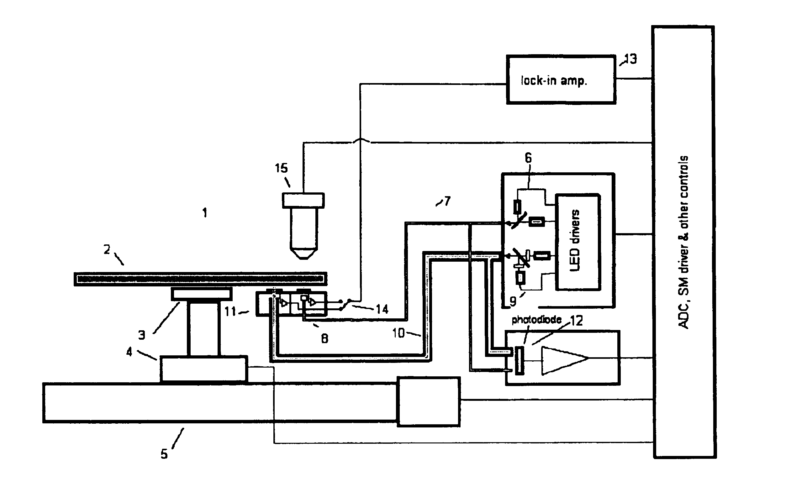
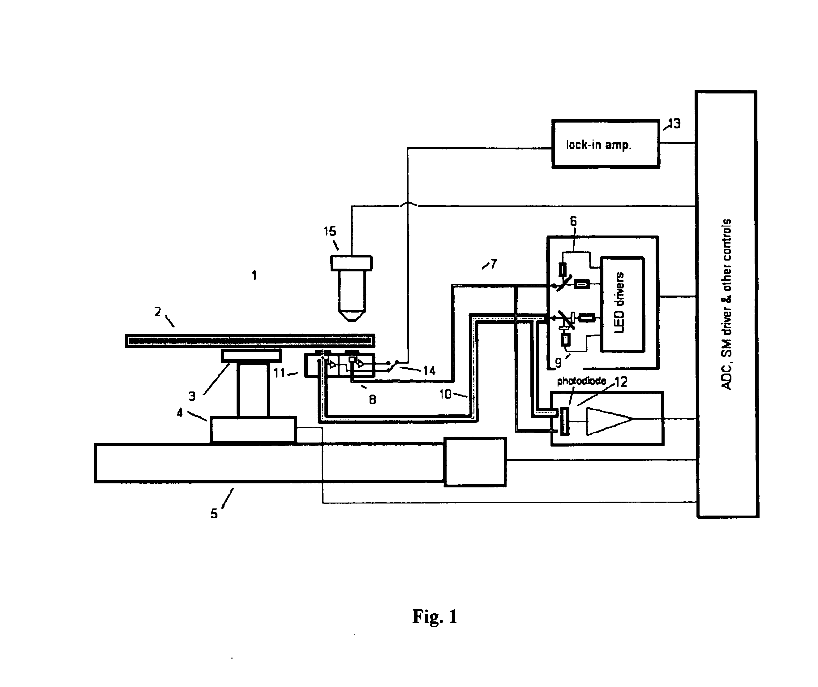
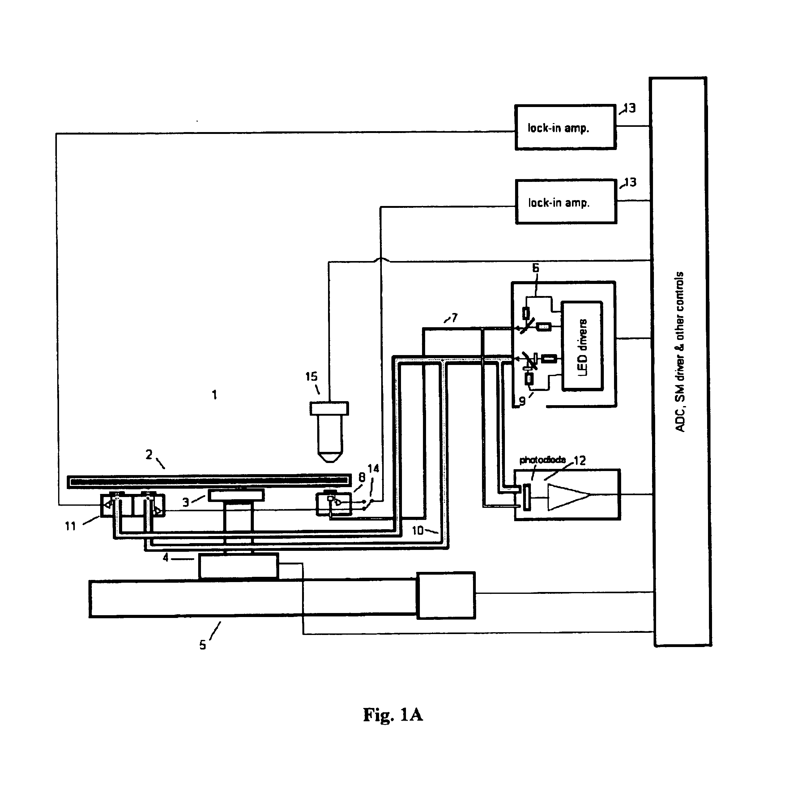
[0027]Referring to FIGS. 1, 1A, 1B, 2, 3, 4, an apparatus 1 is shown for determining minority carrier diffusion length of a semiconductor wafer 2. Briefly, the apparatus includes a grounded chuck 3 with diameter less than the diameter of the silicon wafer 2. The wafer chuck 3 is mounted on the rotary stage 4 and linear stage 5. For measurement in the central region the position of the wafer on the chuck is changed using robotic or other system. The apparatus also includes optical and electrical components, which give possibility to illuminate the back surface of the wafer and detect the surface photo voltage on the back surface. A first source of the light 6 consists of two or more laser LED's installed in the optical combiners. A first source of the photons 6 is coupled through first optical fiber system 7 to first SPV transducer 8 to direct light onto back surface of the wafer. A second source of the photons 9 consists of two or more LED's with interference opt...
PUM
 Abstract
Description
Claims
Application Information