Flat panel display device and method of forming passivation film in the flat panel display device

a flat panel display and display device technology, applied in the manufacture of electrode systems, cold cathode manufacturing, electric discharge tube/lamp manufacture, etc., can solve the problems of easy deformation, effect on the lifetime of the device, and organic light-emitting devices, and achieve good characteristic and simple process

Inactive Publication Date: 2005-08-09
UNILOC 2017 LLC
View PDF10 Cites 49 Cited by
  • Summary
  • Abstract
  • Description
  • Claims
  • Application Information

AI Technical Summary

Benefits of technology

[0017]Another object of the present invention is to manufacture a passivation film having a good characteristic through simple process.

Problems solved by technology

As described above, the organic light-emitting device has disadvantages that it is easily degraded by internal factors such as degradation of the cathode electrode due to oxygen, degradation of the light-emitting layer due to oxygen from ITO, degradation due to reaction between the light-emitting layer and the interface or the like, and by external factors such as moisture, oxygen, ultraviolet rays, manufacture conditions of the device, and the like.
In particular, packaging of the organic light-emitting device is very important since external oxygen and moisture give a fatal effect on the lifetime of the device.
However, this conventional method discloses only a high temperature process, which is useful for the fabrication of dielectric thin film having high breakage strength and a low leakage current.
As described above, the methods of fabricating the inorganic insulating film according to the prior arts have disadvantages that the deposition temperature is relatively high, the step coverage of the thin film is poor and the density thereof is not good.

Method used


Image

  • Flat panel display device and method of forming passivation film in the flat panel display device
  • Flat panel display device and method of forming passivation film in the flat panel display device
  • Flat panel display device and method of forming passivation film in the flat panel display device

Examples


embodiment 1

[0031](Embodiment 1)

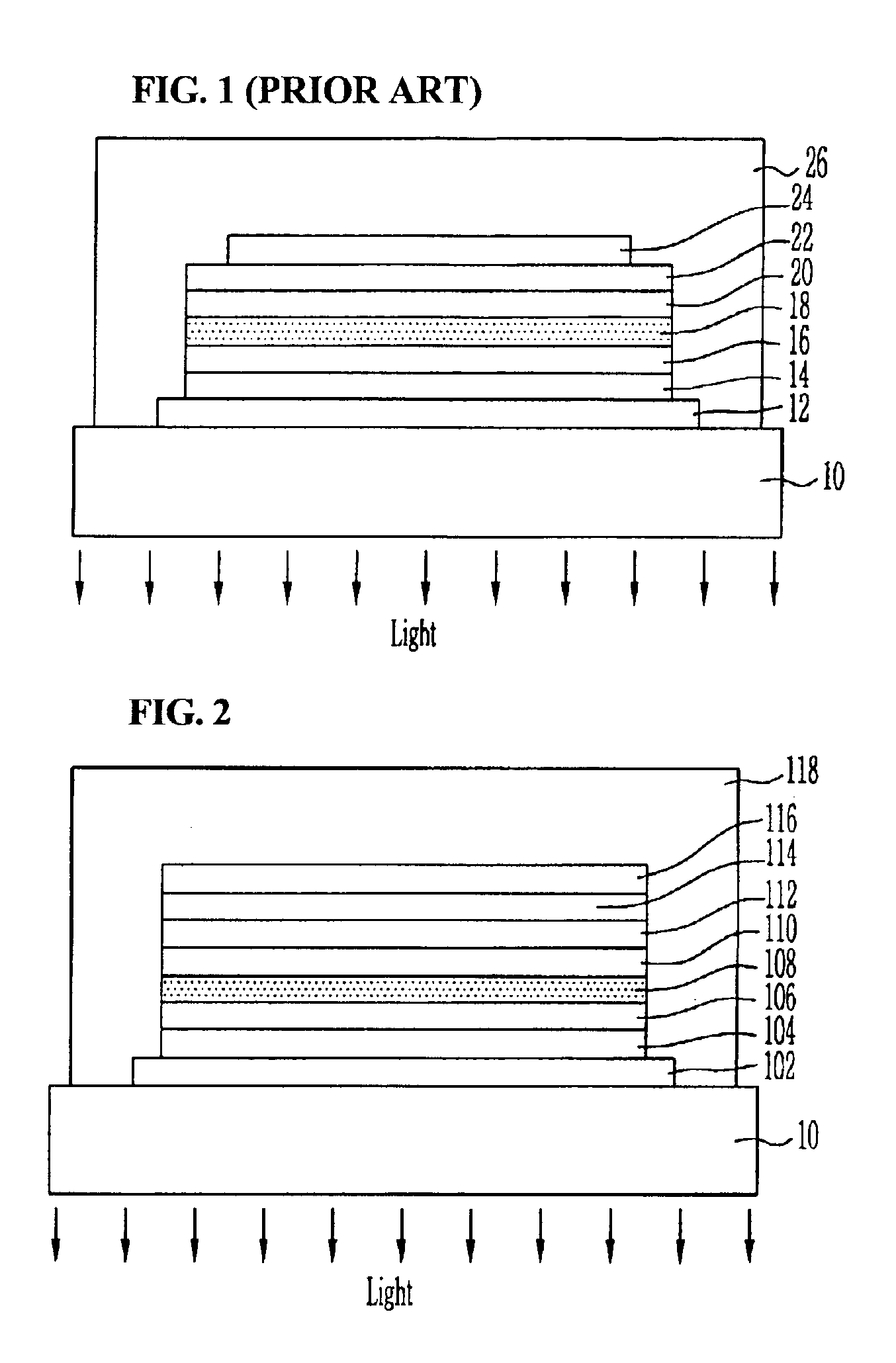
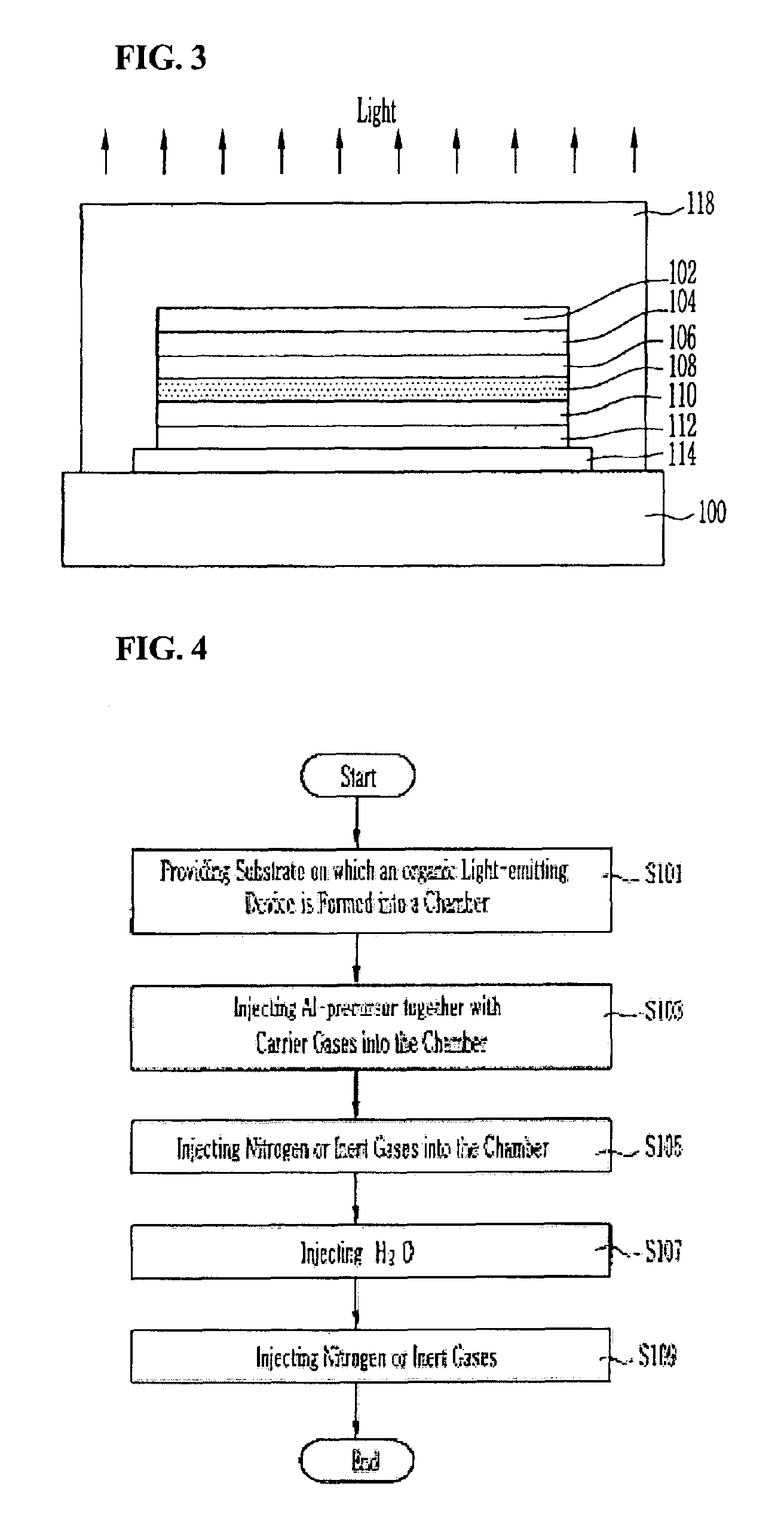
[0032]FIG. 2 is a cross-sectional view of an organic light-emitting device for explaining a method of forming a passivation film in the organic light-emitting device according to the embodiment 1 of the present invention. FIG. 2 shows an organic light-emitting device in which emitted lights penetrate a transparent substrate.

[0033]Referring now to FIG. 2, the organic light-emitting device has a structure in which an anode electrode 102, a hole injection layer 104, an hole transporting layer 106, a light-emitting layer 108, an electron transporting layer 110, an electron injection layer 112 and a cathode electrode 114 are stacked on a transparent substrate 100. The transparent substrate 100 may be made of a glass substrate or a plastic substrate.

[0034]In order to passivate the organic light-emitting device, a metal film 116 is formed on the cathode electrode 114. The metal film 116 may be made of Al or a transition metal that is more insensitive to oxygen or moistu...

second embodiment

[0061](Second Embodiment)

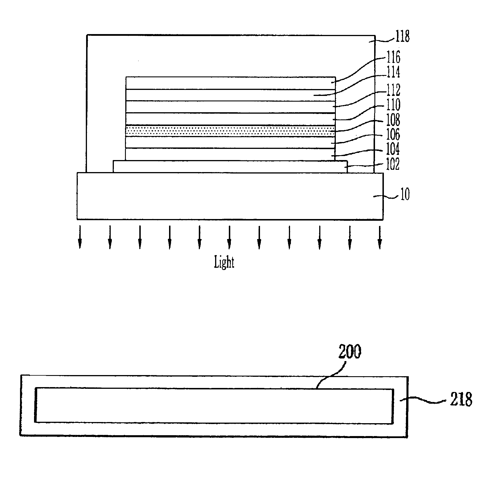
[0062]FIG. 3 is a cross-sectional view of the organic light-emitting device for explaining a method of forming the passivation film in the organic light-emitting device according to the second embodiment of the present invention. FIG. 3 is a cross-sectional view of the organic light-emitting device of the top emission mode (light is emitted toward the upper side).

[0063]Unlike the organic light-emitting device shown in FIG. 2, the organic light-emitting device of the second embodiment has a cathode electrode 114, an electron injection layer 112, an electron transporting layer 110, a light-emitting layer 108, a hole transporting layer 106, a hole injection layer 104 and an anode electrode 102, all of which are stacked on a non-transparent substrate 200 of Si, etc., so that light is emitted toward an upper side. Another top emission type of organic light-emitting device has a transparent upper metal electrode. This organic emitting device may have a structure i...


PUM

PropertyMeasurementUnit
temperatureaaaaaaaaaa

Abstract

A method of forming a passivation film in a flat panel display device includes forming the flat panel display device on a substrate, bringing the flat panel display device into a chamber in order to form the passivation film, injecting precursors containing constituent elements of the passivation film into the chamber where the precursors include at least oxygen plasma, ammonia plasma, or nitrogen plasma, and forming the passivation film of an inorganic insulating material at a temperature of 20-220° C. through a surface chemical reaction between the precursors by a plasma enhanced atomic layer deposition method.

Description

BACKGROUND OF THE INVENTION[0001]1. Field of the Invention[0002]The invention relates to a flat panel display device and a method of forming a passivation layer in the flat panel display device. More particularly, it relates to a method of forming a passivation layer deposited by means of an atomic layer deposition method through a surface chemical reaction between precursors, which include atomic elements of the passivation layer.[0003]2. Description of the Prior Art[0004]With an advent of 21st century of higher information era, researches and developments on a next-generation display device have increasingly been important. In particular, the development of materials for use in display devices for communications and computers is important and will be more important in the future. Among the flat panel displays, an organic electroluminescence (OEL) device or an organic light-emitting device (OLED) bears particular significance, because the display devices offer self-emitting lights....

Claims


Application Information

Patent Timeline
Patent Type & Authority Patents(United States)
IPC IPC(8): H01L51/52H01L51/50C23C16/44C23C16/455
CPCC23C16/45525H01L51/5253H01L51/5256H10K50/8445H10K50/844
Inventor PARK, SANG HEEYUN, SUN JINKIM, YOUNG SHINLEE, YONG EUI
Owner UNILOC 2017 LLC
Why Eureka
Try Eureka