

Method of producing semiconductor device
a semiconductor and production method technology, applied in the direction of crystal growth process, polycrystalline material growth, chemistry apparatus and processes, etc., can solve the problems of insufficient effect of method and insufficient crystallization of amorphous silicon film, and achieve low cost, high yield, and less variation in properties
- Summary
- Abstract
- Description
- Claims
- Application Information
AI Technical Summary
Benefits of technology
Problems solved by technology
Method used
Image

Examples
first embodiment
[First Embodiment]
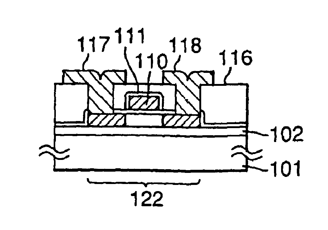
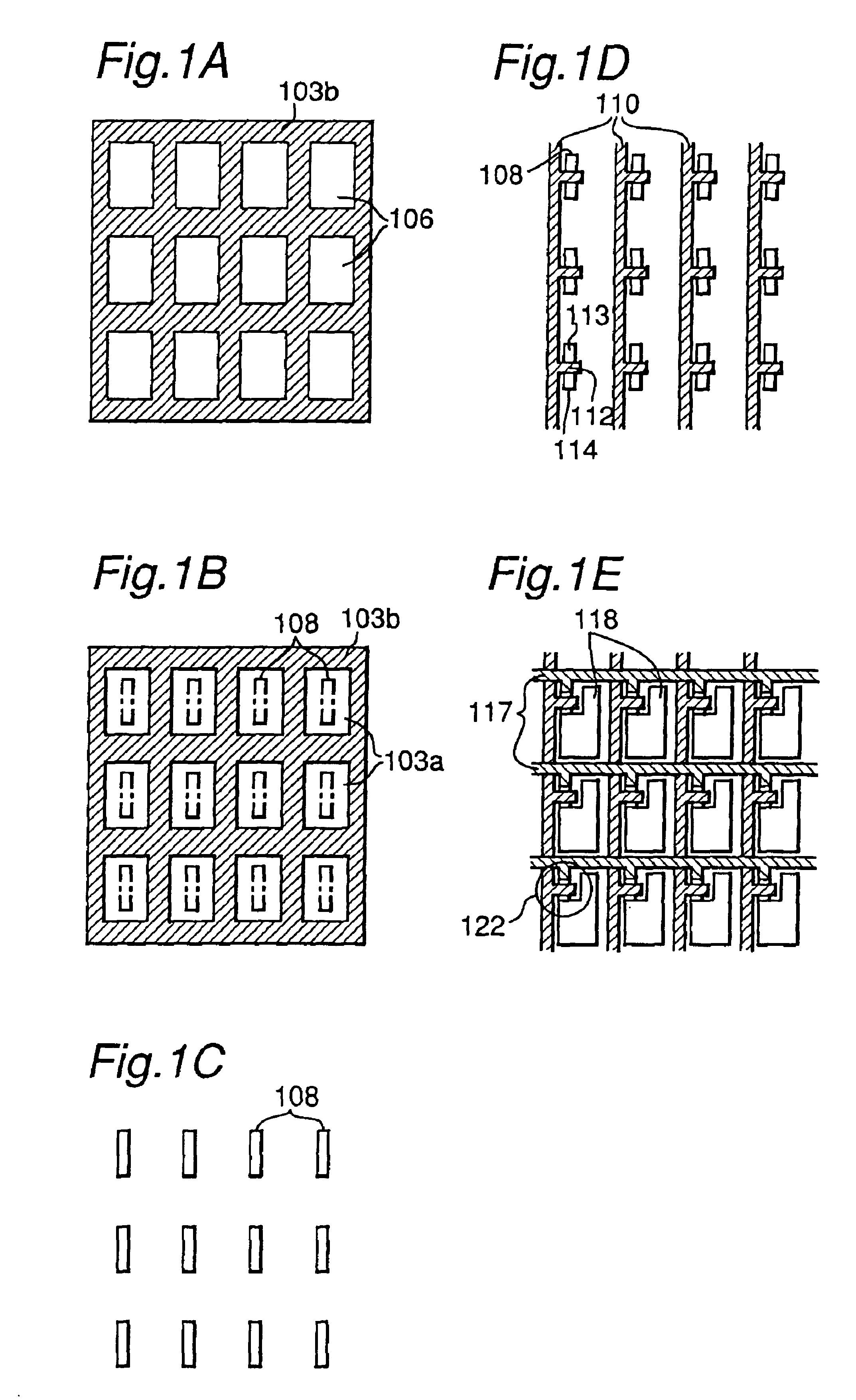
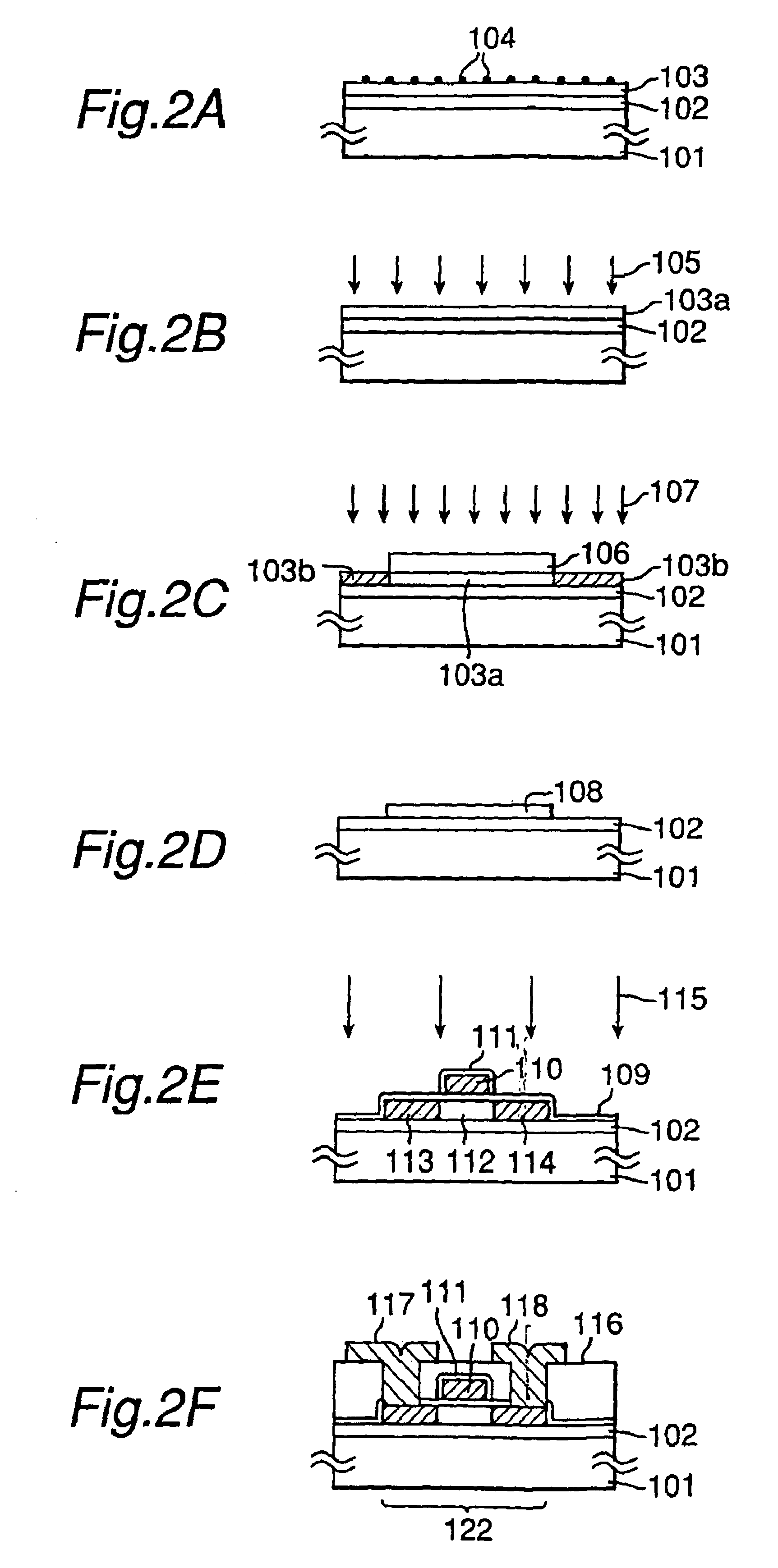
[0072]The first embodiment of the manufacturing method of a semiconductor device of the present invention will be described. In the first embodiment, the present invention is utilized in a process for fabricating N-type TFTs on a glass substrate. The TFTs that are fabricated in this embodiment can be used not only for a driver circuit and pixels of an active matrix type liquid crystal display device, but also as elements constituting a thin film integrated circuit. In this embodiment, as a representative of these, pixel-driving TFTs of an active matrix substrate for a liquid crystal display device, which particularly requires uniform fabrication of several hundred thousands to several millions of N-type TFTs, are taken and described.
[0073]Plan views of pixel TFTs on the active matrix substrate being produced in the first embodiment are shown in FIGS. 1A, 1B, 1C, 1D and 1E according to the order of the fabrication steps. In reality, the active matrix substrate has a...
second embodiment
[Second Embodiment]
[0090]Next, referring to FIG. 3 and FIGS. 4A-4F, a second embodiment of the present invention will be described. The production method according to the second embodiment is applied to the steps of fabricating on a quartz glass substrate a CMOS circuit in which N-type TFTs and P-type TFTs are formed complementarily. These TFTs will constitute peripheral drive circuits of active matrix type liquid crystal display devices and general thin film integrated circuits.
[0091]FIG. 3 is a plan view showing the outline of the TFT fabrication process steps in this second embodiment. FIGS. 4A-4F: are cross-sectional views taken along the line IV—IV of FIG. 3, in which the fabrication steps sequentially proceeds in the order of the figures.
[0092]First, as shown in FIG. 4A, on a quartz glass substrate 201, an undercoat film 202 made of silicon oxide is formed to a thickness of about 300-500 nm by a CVD method. Then, a minute amount of nickel 204 is added to the surface of the und...
PUM
| Property | Measurement | Unit |
|---|---|---|
| size | aaaaa | aaaaa |
| grain size | aaaaa | aaaaa |
| temperature | aaaaa | aaaaa |
Abstract
Description
Claims
Application Information