
Vacuum deposition of dielectric coatings on volatile material

a dielectric coating and volatile material technology, applied in vacuum evaporation coatings, coatings, instruments, etc., can solve the problems of difficult vacuum coating of materials that have a tendency to evaporate and decompose under vacuum, mechanical instability, and extremely low yield in manufacturing,

Inactive Publication Date: 2005-08-23
PHOTON DYNAMICS
View PDF12 Cites 1 Cited by
  • Summary
  • Abstract
  • Description
  • Claims
  • Application Information

AI Technical Summary

Benefits of technology

[0012]While the principal advantage of this invention is the prevention of evaporation and of breakdown of the water-based emulsion so that coatings can be applied under vacuum, a further advantage of the invention is the elimination of all manual handling-related processing errors, thus improving the overall yield. It also improves optical quality by elimination of air bubbles between the dielectric coating and PDLC layer due to very high adhesion and conformal coating of dielectric thin films. It is estimated that overall manufacturing cost of the EO modulator is reduced by at least 75%.
[0013]The invention will be better understood by reference to the following detailed description in connection with illustrations of specific embodiments.

Problems solved by technology

One of the challenges of manufacturing is the difficulty of vacuum coating of materials that have a tendency to evaporate and decompose under vacuum.
The lamination process has the limitation of inconsistent surface flatness, mechanical instability, and extremely low yield in manufacture.
While the mirror surface directly engages the light sensitive material, representing an improvement over prior art techniques, the assembly process is subject to human-introduced errors such as wrinkling of the pellicle, nonuniform adhesion, capture of dust particles and creation of bumps at the time of assembly.

Method used


Image

  • Vacuum deposition of dielectric coatings on volatile material
  • Vacuum deposition of dielectric coatings on volatile material

Examples


Embodiment Construction

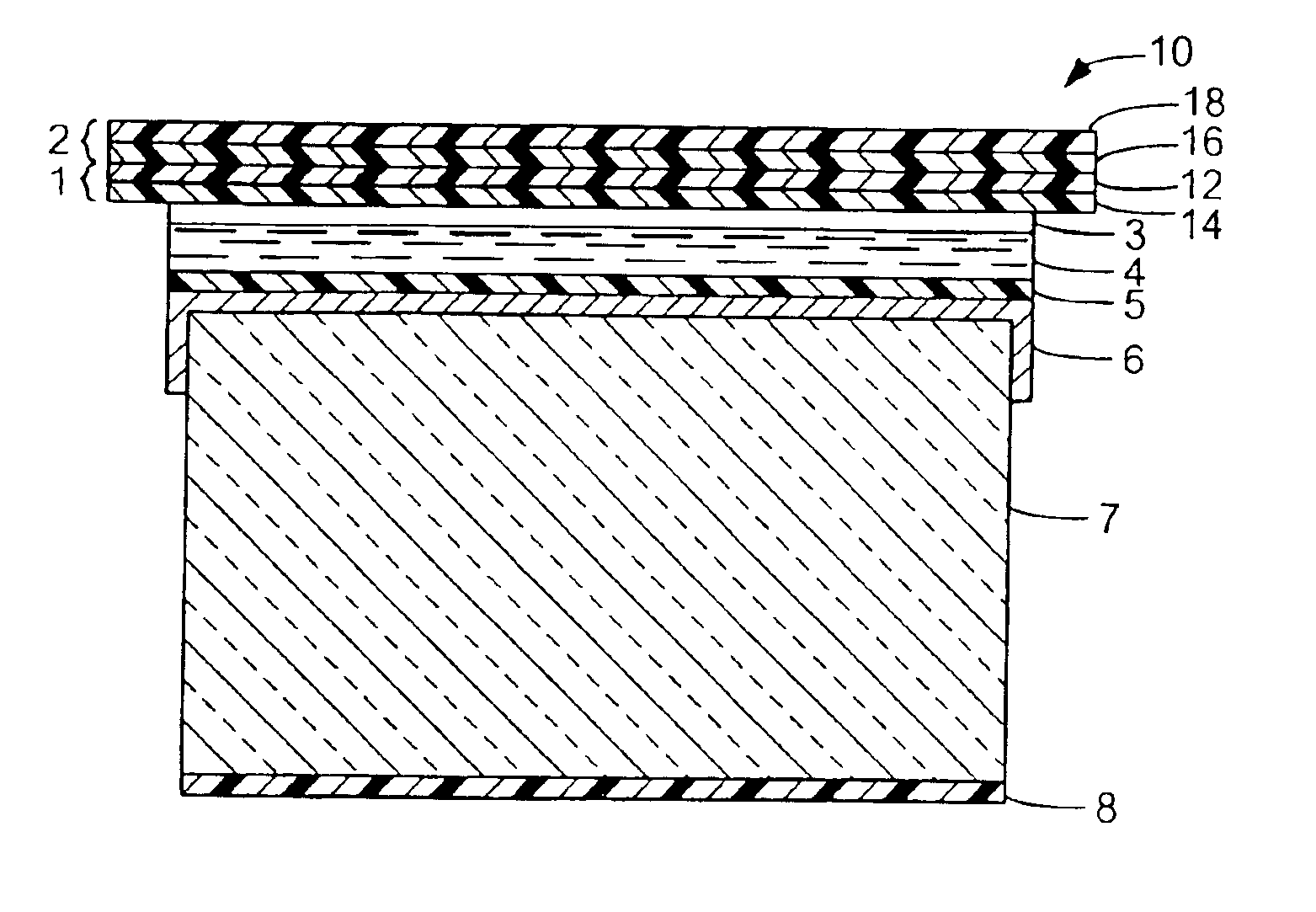
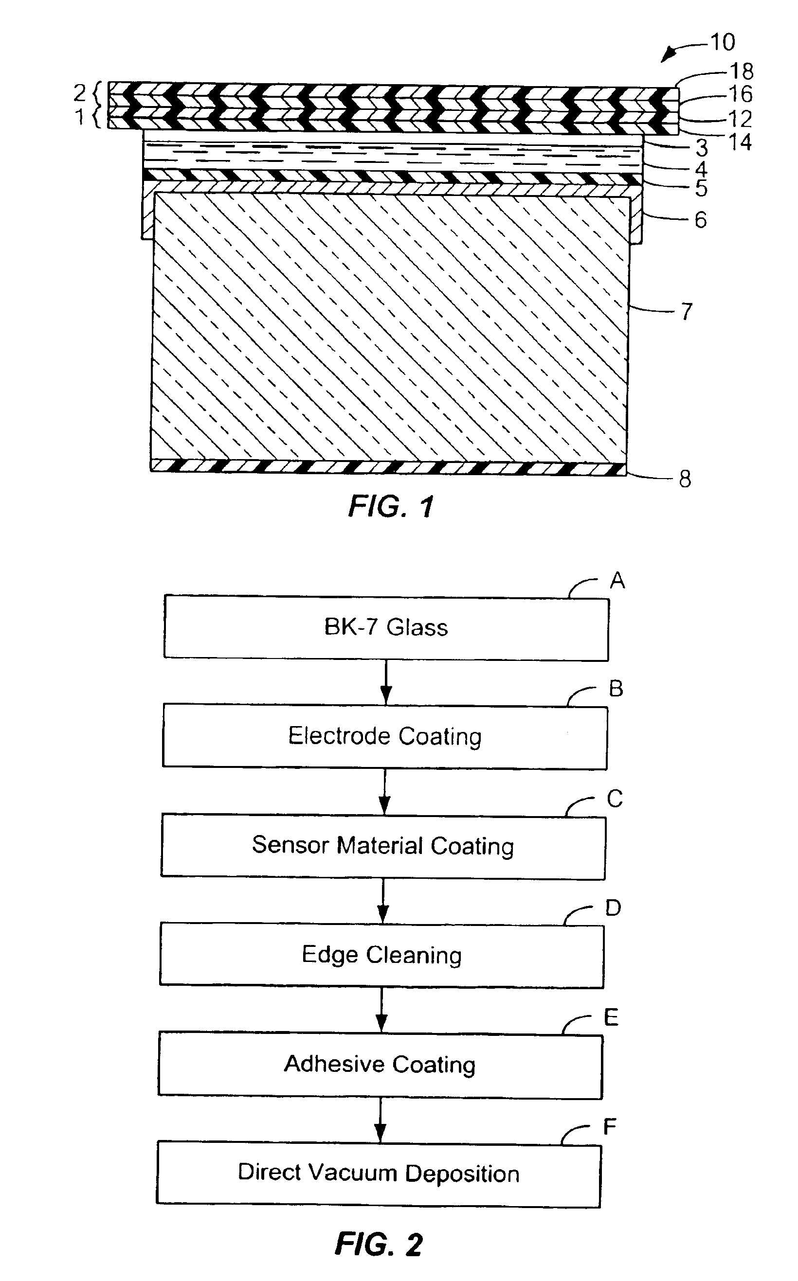
[0016]Referring to FIG. 1, there is shown a schematic cross-sectional view of an electro optic modulator device 10 manufactured according to the invention. This is only one example of a device manufactured according to this process.

[0017]In an optical element application, EO modulator 10 has at least two pairs 1, 2 of thin dielectric materials 12, 14, 16, 18 of alternately high and low index of refraction overlay a stress-absorptive polymeric adhesive layer 3. The polymer adhesive layer 3 has distinct characteristics as will be explained. The pairs 1, 2, which are not shown to scale, are bonded via the stress-absorptive polymeric adhesive layer 3 on a layer of volatile gelatinous material 4, specifically in an optical application, polymer dispersed liquid crystal (PDLC), which serves as the sensor material 4. The sensor material 4 rests on an optional layer of silicon dioxide 5. Thereunder is a layer of a transparent electrode material 6, such as indium tin oxide (ITO) which in turn...


PUM

PropertyMeasurementUnit
pressureaaaaaaaaaa
reflectivityaaaaaaaaaa
thicknessaaaaaaaaaa

Abstract

In order to allow application of any coating under a vacuum over a volatile gelatinous layer, such as polymer dispersed liquid crystal (PDLC) on an optical glass substrate with a transparent electrode, such as indium tin oxide (ITO) on its surface, a layer of an intermediate stress absorbing polymeric material is first applied to cover the volatile gelatinous layer to prevent evaporation and escape of volatiles, thereafter the coating is applied under a very high vacuum using for example a technique called Physical Vapor Deposition (PVD) or sputtering.

Description

CROSS-REFERENCES TO RELATED APPLICATIONS[0001]Not ApplicableSTATEMENT AS TO RIGHTS TO INVENTIONS MADE UNDER FEDERALLY SPONSORED RESEARCH OR DEVELOPMENT[0002]Not ApplicableREFERENCE TO A “SEQUENCE LISTING,” A TABLE, OR A COMPUTER PROGRAM LISTING APPENDIX SUBMITTED ON A COMPACT DISK[0003]Not ApplicableBACKGROUND OF THE INVENTION[0004]This invention relates to methods for applying coatings to volatile gelatinous surfaces on substrates in a high vacuum, and more particularly this invention relates to thin film deposition of dielectric on liquid crystal on a substrate with specific application to deposition of multilayer optical quality dielectric materials on polymeric liquid crystal materials for use in electro-optic applications.[0005]One of the challenges of manufacturing is the difficulty of vacuum coating of materials that have a tendency to evaporate and decompose under vacuum. One material of interest is polymer dispersed liquid crystal (PDLC) film, the material used in electro-o...

Claims


Application Information

Patent Timeline
Patent Type & Authority Patents(United States)
IPC IPC(8): C23C14/02G02F1/13G02F1/1334C25D2/00G02F1/1335
CPCC23C14/024G02F1/1334G02F1/133516G02F1/133553G02F2001/133521G02F1/133521C23C14/02C23C14/00C23C14/24
Inventor PETHE, RAJIVGUPTA, PRAMODCHEN, XIANHAINAGY, ALEXANDER
Owner PHOTON DYNAMICS
Learn More