Systems for programmable memory using silicided poly-silicon fuses

a polysilicon fuses and programmable memory technology, applied in semiconductor devices, digital storage, instruments, etc., can solve the problems of affecting the reliability of the programmed fuse, the programmed fuse is prone to contamination through the passivation window opening, and the manufacturing technique of non-volatile memory increases the complexity and chip siz

Inactive Publication Date: 2005-08-23
AVAGO TECH WIRELESS IP SINGAPORE PTE
View PDF2 Cites 39 Cited by
  • Summary
  • Abstract
  • Description
  • Claims
  • Application Information

AI Technical Summary

Problems solved by technology

The non-volatile memory manufacturing techniques increase the complexity and chip size.
One of the disadvantages of this method is that the programmed fuse is prone to contamination through the passivation window opening.
Furthermore, the need for high voltages to be internally generated to create such high currents can impact reliability of the programmed fuse and integrity of underlying oxide layers in sub-micron CMOS processing, which cannot tolerate high programming voltages.
Due to this reliability hazard, the unpredictability of post-programming resistance of the fuse also increases.

Method used


Image

  • Systems for programmable memory using silicided poly-silicon fuses
  • Systems for programmable memory using silicided poly-silicon fuses
  • Systems for programmable memory using silicided poly-silicon fuses

Examples


Embodiment Construction

[0045]

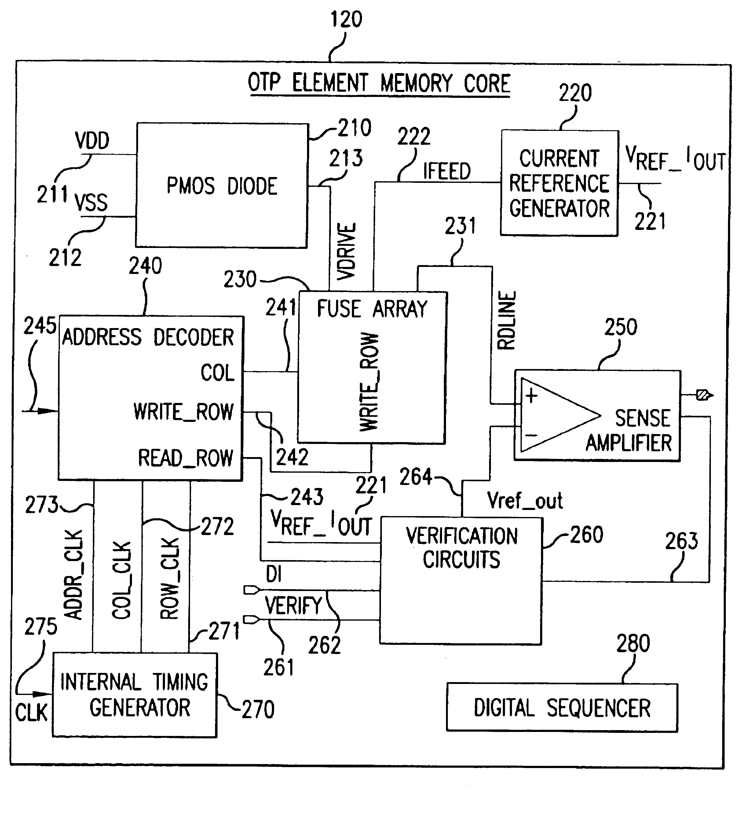
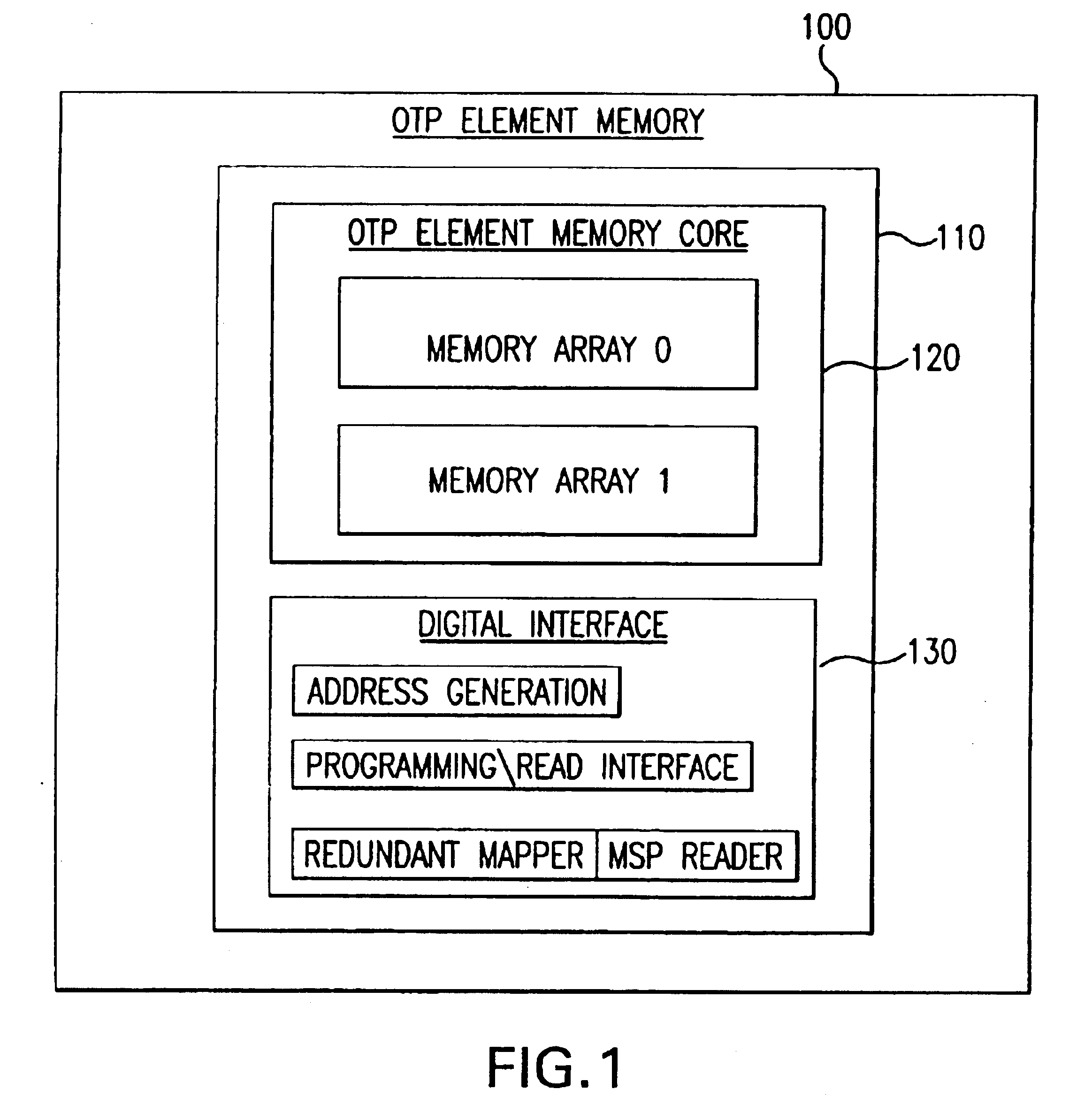
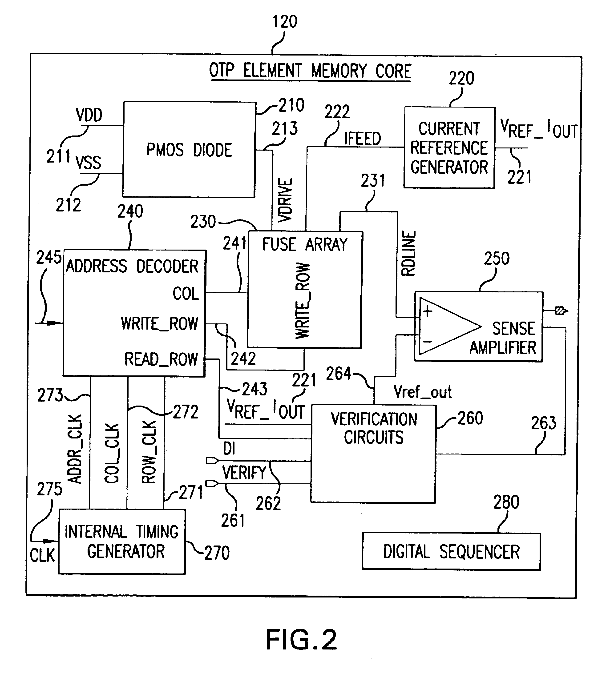
Table of Contents.1.Introduction.2.One-Time Programmable (OTP) Memory Element - SystemStructure.a. OTP Memory Core.b. Row-column Matrix Memory Array Scheme.c. Address Decoder.d. Internal Timing Generator.e. Verification Circuit.f. PMOS Diode.3.OTP Memory Element in - System Operation.a. Programming Mode.b. Reading Mode.c. Verification mode.4.Poly-Si Fuse Design.5.Conclusion.

[0046]While the present invention is described herein with reference to illustrative embodiments for particular applications, it should be understood that the invention is not limited thereto. Those skilled in the art with access to the teachings provided herein will recognize additional modifications, applications, and embodiments within the scope thereof and additional fields in which the present invention would be of utility.

1. Introduction.

[0047]The present invention relates to semiconductor programmable elements. In particular, the present invention is directed to a one-time programmable (“OTP”) memory...


PUM


Abstract

The present invention is directed to systems for evaluating one-time programmable memory cells. A threshold current is applied to a resistive circuit, thereby generating a threshold voltage. A read current is applied to a first memory cell, thereby generating a memory cell voltage. The memory cell voltage is compared to the threshold voltage, thereby determining the state of the memory cell. In a further embodiment of the invention, a second threshold voltage is generated and compared the memory cell voltage, thereby verifying the state of the memory cell. The threshold current is optionally a substantial replica of said read current. The threshold current is optionally a proportional substantial replica of said read current. In an embodiment, the resistive circuit includes a second memory cell, which can be programmed or unprogrammed. The second memory cell is optionally arranged to average the memory cell resistance.

Description

CROSS-REFERENCE TO RELATED APPLICATIONS[0001]This application is a continuation of U.S. application Ser. No. 10 / 355,237, titled, “Methods and Systems for Programmable Memory Using Silicided Poly-Silicon Fuses,” filed Jan. 31, 2003 now U.S. Pat. No. 6,798,684 (allowed), which is a continuation-in-part of U.S. application Ser. No. 10 / 115,013, titled, “An Integrated Fuse with Regions of Different Doping,” filed Apr. 4, 2002 (U.S. Pat. No. 6,580,156), issued Aug. 12, 2004 and which claims the benefit of U.S. Provisional Patent Application No. 60 / 377,238, filed May 3, 2002, all of which are incorporated herein by reference in their entireties.BACKGROUND OF THE INVENTION[0002]1. Field of the Invention[0003]The present invention is directed to semiconductor fuses and systems for evaluating semiconductor fuses.[0004]2. Background Art[0005]In the field of data storage, there are two main types of storage elements. The first type is volatile memory that has the information stored in a particu...

Claims


Application Information

Patent Timeline
Patent Type & Authority Patents(United States)
IPC IPC(8): G11C7/00G11C17/00G11C5/00
CPCH01L23/5256H01L2924/0002H01L2924/00
Inventor LOW, KHIM L.BROOKS, TODD L.WOO, AGNESITO, AKIRA
Owner AVAGO TECH WIRELESS IP SINGAPORE PTE
Why Eureka
Try Eureka