

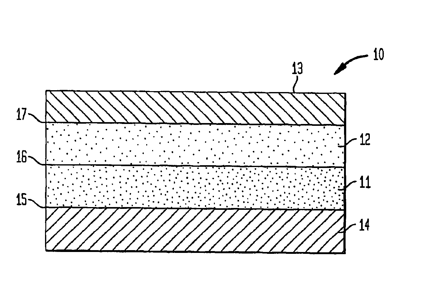
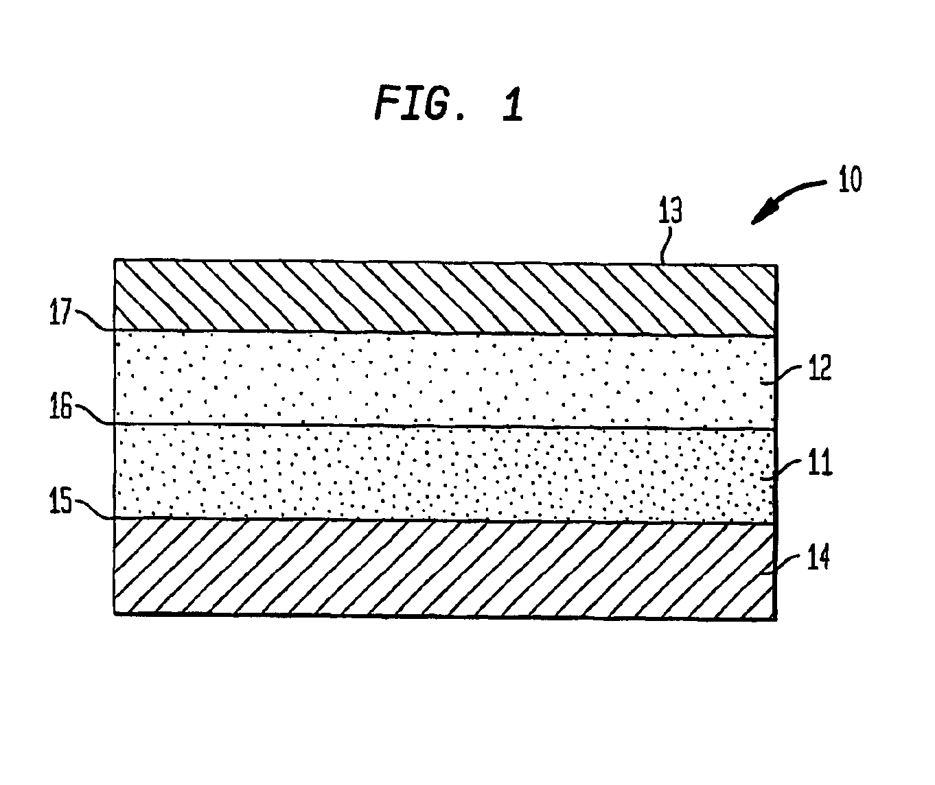
MIS hydrogen sensors
a hydrogen sensor and sensor technology, applied in the field of gas sensors, can solve the problems of inability to identify the source or the location of hydrogen leakage, most, if not all, known hydrogen sensors have not entered commercial production, and are considerably more difficult to achiev
- Summary
- Abstract
- Description
- Claims
- Application Information
AI Technical Summary
Benefits of technology
Problems solved by technology
Method used
Image

Examples
example 1
[0045]In a particular illustrative embodiment, Pd / AlN / Si MIS hydrogen sensor devices were fabricated by PSMBE in order to assure epitaxial growth of the insulating AlN layer. The Si substrate was siliconN-type with specified low resistivity, and a thickness of about 380±20 mm.
[0046]The base pressure of the ultrahigh vacuum PSMBE system was 7.3×10⁻⁹ TORR, and during deposition, the dynamic pressure was maintained constant at 3.5×10⁻³ TORR. The process gases were maintained at a constant flow of 40 sccm of argon (Ar) and 10 sccm of nitrogen (N2). The substrate temperature was kept constant at 650° C. during the entire 10 hour period required to deposit AlN on the substrate to the desired thickness. An acceleration bias of 10 eV was applied to the substrate.
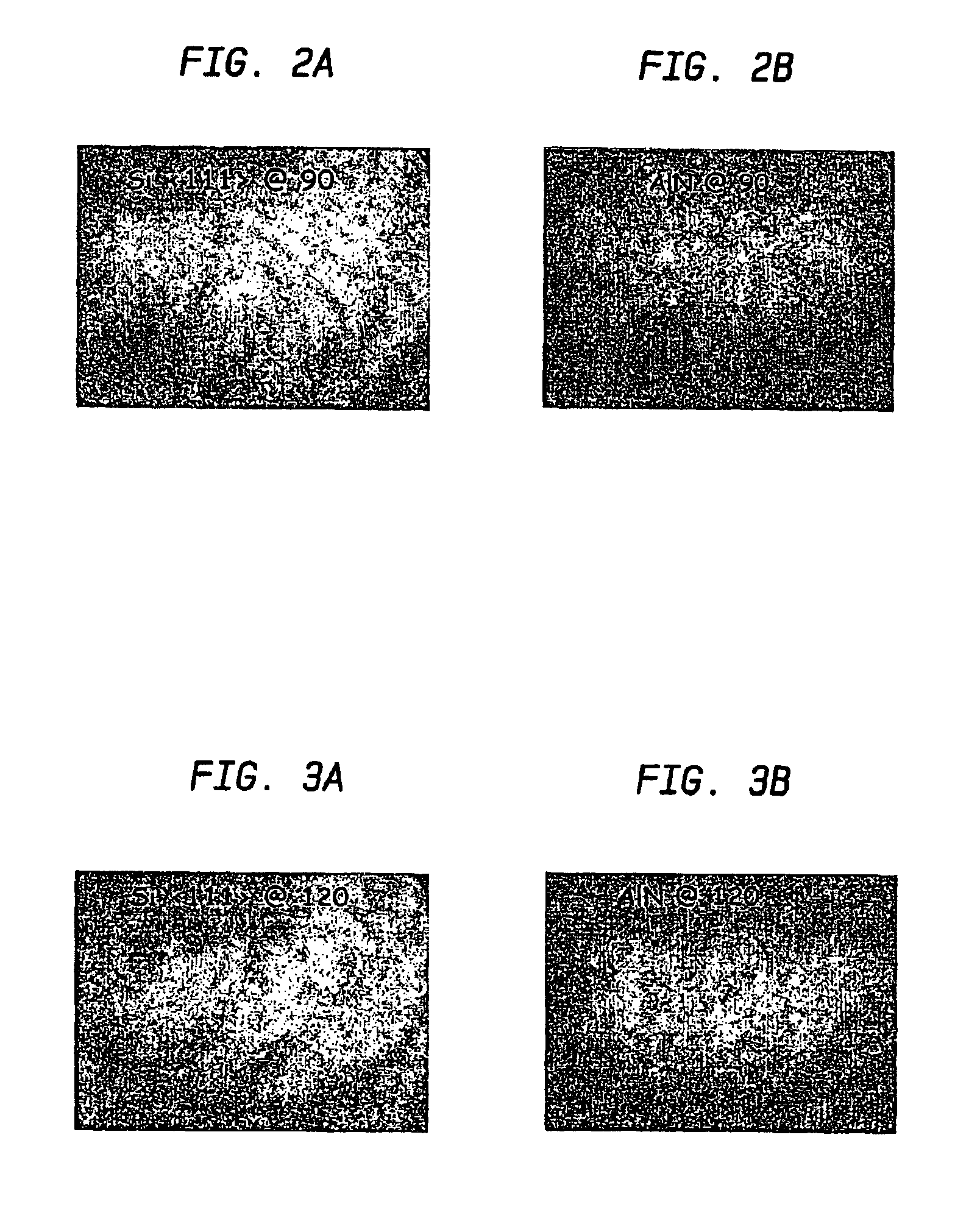
[0047]Optical null ellipsometry of the AlN substrate on the Sisubstrate measured the thickness of the AlN layer and the index of refraction. Devices having different AlN layer thicknesses of (e.g., 700 Å and 1200 Å) were characteriz...
example 2
[0050]In a second specific illustrative embodiment, a Pd / ALN / SiC MIS hydrogen sensor (see, Table 2, Device No. 5) was fabricated by depositing an epitaxial layer of AlN on a standard n-type 6H—SiC wafer by PSMBE under process conditions described above in Example 1. RHEED images (not shown) were obtained before and after the deposition of the AlN on the 6H—SiC wafer to insure epitaxial growth. In this specific embodiment, the epitaxial layer of AlN was 1600 Å thick. A Pd gate layer was deposited on the SiC-based structure to a thickness of 1000 Å. The back contact to the semiconductor substrate, in the SiC-based embodiment, was Pt sputtered to a thickness of 1500 Å.
[0051]Table 2 summarizes the devices fabricated in accordance with Examples 1 and 2:
[0052]
TABLE 2TABLE 1: INSULATOR AND CATALYST THICKNESSDeviceSubstrateAlN Thickness (Å)Pd Thickness (Å)1Si 70010002Si 120010003Si 70020004Si 1200200056H-SiC16001000
Experimental Results:
[0053]The tests required for electrical characterizatio...
PUM
| Property | Measurement | Unit |
|---|---|---|
| temperature | aaaaa | aaaaa |
| thickness | aaaaa | aaaaa |
| temperature | aaaaa | aaaaa |
Abstract
Description
Claims
Application Information