Optical link module, optical interconnection method, information processor including the optical link module, signal transfer method, prism and method of manufacturing the prism

a technology of optical interconnection and optical link module, applied in the field of information transmission, can solve the problems of large number of channels of optical link modules, high assembly cost, and individual components being required to be extremely compact, and achieve the effects of effective reduction of particularly crosstalk, high efficiency, and improved coupling efficiency

Inactive Publication Date: 2005-09-20
IBM CORP
View PDF16 Cites 21 Cited by
  • Summary
  • Abstract
  • Description
  • Claims
  • Application Information

AI Technical Summary

Benefits of technology

[0026]As a result of detailed studies on the above-described deficiencies and shortcoming of the prior art, we have determined that crosstalk between channels is mainly caused by spherical aberrations on surfaces of lenses, which corresponds to an incident laser beam. In the present invention, a multichannel optical link module is configured, which is capable of effectively reducing particularly crosstalks between channels by including respective lenses formed on surfaces of the prism as aspherical lenses and which is capable of connecting light beams with a high efficiency by improving a coupling efficiency for both of a reception channel and a transmission channel.
[0027]The aspherical lens has a surface in which a plurality of spherical lenses are continuously formed. In the aspherical lens, an outer portion has a spherical surface with a large radius and an inner portion has a spherical surface with a small radius. The above-described configuration reduces the crosstalk between channels while achieving a short focal length required miniaturization and further obtains a high connection efficiency. Furthermore, the optical link module of the present invention provides a high-speed wiring element which is excellent in flexibility and in stability for a heat property in an information processor.

Problems solved by technology

However, conventional optical link modules are mainly for middle- / long-distance applications such as the Internet and a telephone system and thus the number of channels thereof is overwhelmingly smaller than that of an optical link module used for a computer.
In assembly thereof, alignment of an optical axis, referred to herein as “active alignment”, is always required and thus an assembly cost becomes high.
However, in order to realize high-density packaging on a circuit board, individual components are required to be extremely compact.
Thus, racks for arranging a number of circuit boards are bulky and it is difficult to meet requests, such as for the miniaturization of an information processor and the saving of space therein.
Furthermore, a link method using the flexibility of the above-described optical fiber has an inconvenience that it is impossible to achieve speeding-up by shortening a signal transmission distance by high-density packaging, which is an original aim.
However, the optical link module disclosed in Japanese Patent Laid-Open No. 2001-242358 has a problem that an electrically bendable wiring pattern cannot be formed.
Furthermore, a method of connecting the LD / PD to four sides of the IC in a space by bending the flexible cable so as to surround the space has assembly problems and poor high-frequency properties.
Accordingly, if the conventional technology is applied as it is, there is a difficulty that the optical element cannot be realized within a range which satisfies imaging conditions of a thick lens.
Even if an attempt is made to solve the above-described problem only by use of a prism without using a lens array, this is not altogether satisfactory.
Specifically, when an optical bend or turn is formed by use of a prism (or a mirror) as it is for a two-dimensional array, there is crosstalk in an adjacent channel as described later and the power of the light beam is greatly lost.
Thus, it is not possible to apply the optical element as it is to the signal wiring element in the information processor.
Even if the pitches of the arranged optical fibers and PDs are increased to grow in size in order to avoid such a crosstalk, the distance through which the luminous flux has to travel is accordingly increased and there arises an inconvenience of a lowered coupling efficiency.
Moreover, when the fiber end, the PD and the LD are separated from the prism, a distance through which light travels in the air (the air has a refractive index of 1, which is lower than that of the prism) is increased and thus there arises an inconvenience that characteristics are more deteriorated.

Method used


Image

  • Optical link module, optical interconnection method, information processor including the optical link module, signal transfer method, prism and method of manufacturing the prism
  • Optical link module, optical interconnection method, information processor including the optical link module, signal transfer method, prism and method of manufacturing the prism
  • Optical link module, optical interconnection method, information processor including the optical link module, signal transfer method, prism and method of manufacturing the prism

Examples


Embodiment Construction

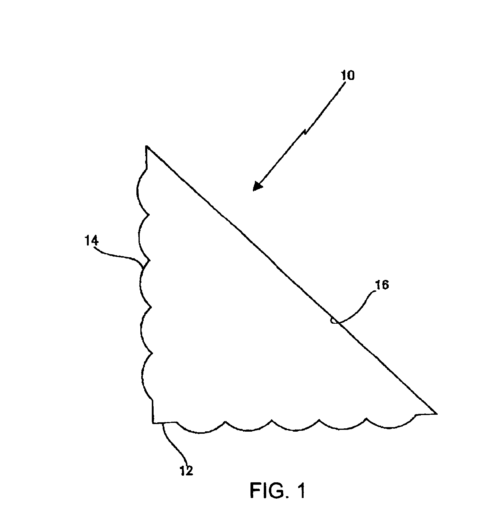
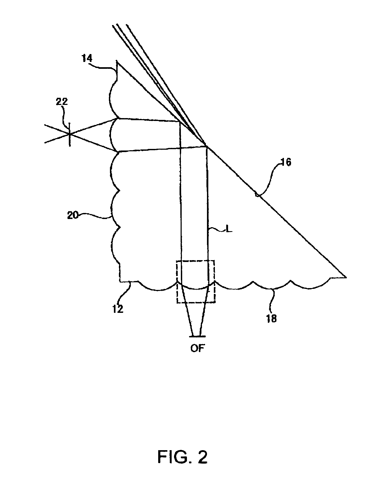
[0053]The present invention will be described below by use of a specific embodiment shown in the drawings. However, the present invention is not limited to the embodiment shown in the drawings. FIG. 1 shows an embodiment of a prism included in an optical link module of the present invention. The prism 10 used in the optical link module of the present invention includes: an incidence plane 12 which gives an optical interface for input / output of a light beam; an output plane 14; and a reflection plane 16 having a function of mainly reflecting the light beam made incident thereon.

[0054]The incidence plane 12 and the output plane 14 are terms used for the sake of simplicity in the description. The prism is configured in such a manner that both of the incidence plane 12 and the output plane 14 can function as the output plane and the incidence plane. Moreover, a material of the prism is not particularly limited in the present invention and various materials can be used, such as quartz gl...


PUM


Abstract

An optical link module of the present invention for connecting light beams by deflection and including light-emitting devices arranged in a planar manner; an optical fiber bundle that is an optical waveguide for receiving the light beams from the light-emitting devices, and an optical turn which includes a plurality of aspherical lenses which are disposed between the light-emitting devices and the optical fiber bundle and are formed while corresponding to the number of the light-emitting devices and the number of optical fibers.

Description

BACKGROUND OF THE INVENTION[0001]The present invention relates to information transmission using light in an information processor. More particularly, the present invention relates to an optical link module capable of linking light beams emitted from light emitting devices with high efficiency in a compact volume, an optical interconnection method, an information processor using the optical link module, a signal transfer method in the information processor, a prism used in the optical link module and a method of manufacturing the prism.[0002]With the recent advancement in information-processing technologies, the capacity and the speed of communication between and within housings of information processors have been dramatically advanced. In the immediate future, a speed of a communication request transmitted from one piece of processor board will exceed 1 Tbps. Accordingly, it is predicted that it will be impossible to load connectors for information communications on a card edge by ...

Claims


Application Information

Patent Timeline
Patent Type & Authority Patents(United States)
IPC IPC(8): G02B6/32G02B6/42G02B6/38G02B6/43H01L31/0232H01L33/00H01L33/08H01L33/58H01S5/022
CPCG02B6/32G02B6/4209G02B6/4214G02B6/4292G02B6/3885G02B6/4249G02B6/43
Inventor SEKIYA, KAZUOFUKUZAWA, TADASHI
Owner IBM CORP
Why Eureka
Try Eureka