Methods for post polysilicon etch photoresist and polymer removal with minimal gate oxide loss

a polysilicon and photoresist technology, applied in the direction of liquid cleaning, electric discharge tube, chemistry apparatus and processes, etc., can solve the problems of ineffective removal of undesirable polymer residues by other corrosive solvents, requiring extensive abatement and environmental control, and nonfunctional circuits, etc., to achieve rapid polymer removal, reduce the effect of etching rate and high selectivity

Inactive Publication Date: 2005-10-18
NOVELLUS SYSTEMS
View PDF13 Cites 30 Cited by
  • Summary
  • Abstract
  • Description
  • Claims
  • Application Information

AI Technical Summary

Benefits of technology

[0012]By including a hydrogen source gas to the microwave-generated plasma or inductively-coupled plasma, it is believed that the atomic fluorine concentration is controlled due to in-situ reaction between hydrogen and fluorine species to produce HF vapor. By cont

Problems solved by technology

Post-etch photoresist and polymer residue removal over polysilicon presents numerous challenges.
Traditional wet chemical cleaning methods which use cleaning solutions such as dilute HF (50:1–1000:1 HF:H2O), “hot Piranha” (90% H2SO4/10% H2O2), and other corrosive solvents are often ineffective at removing all undesirable polymer residues.
This can cause device reliability problems or lead to nonfunctional circuits.
These traditional wet clean methods also have the disadvantage of requiring handling and exposure to corrosive, oxidizing, and strongly acidic media, thus requiring extensive abatement and environmental controls.
Although dry plasma cleaning processes offer an alternative approach to wet chemistry cleaning techniques, oftentimes conventional dry plasma chemistries provide insufficient cleaning, require lengthy process times

Method used


Image

  • Methods for post polysilicon etch photoresist and polymer removal with minimal gate oxide loss
  • Methods for post polysilicon etch photoresist and polymer removal with minimal gate oxide loss
  • Methods for post polysilicon etch photoresist and polymer removal with minimal gate oxide loss

Examples


Embodiment Construction

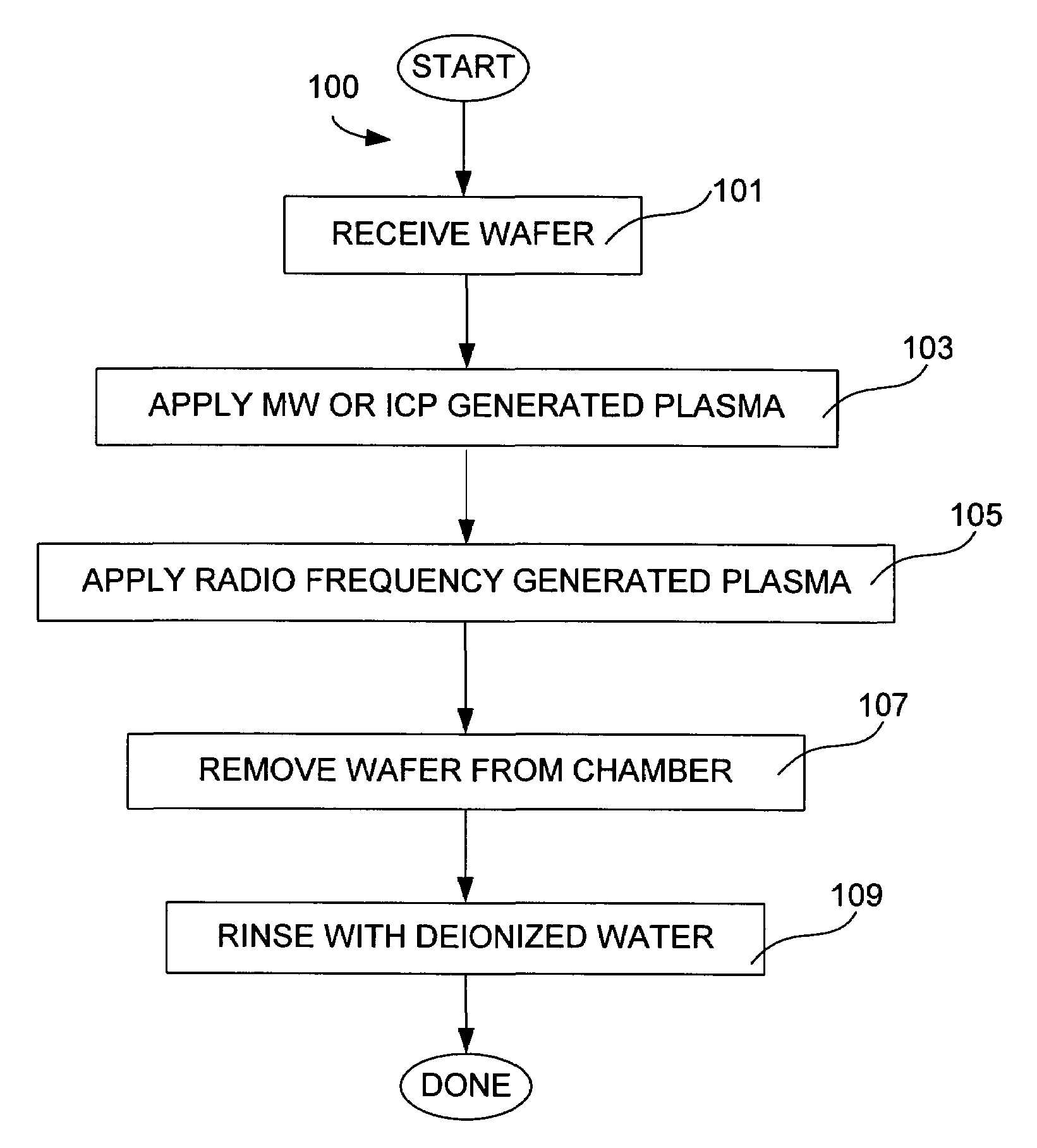
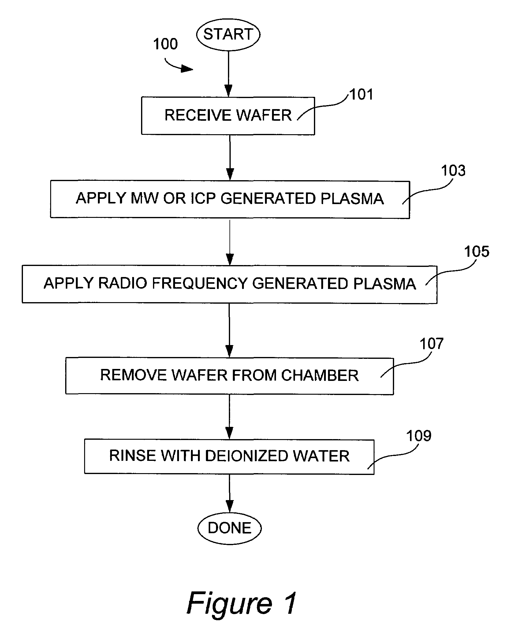
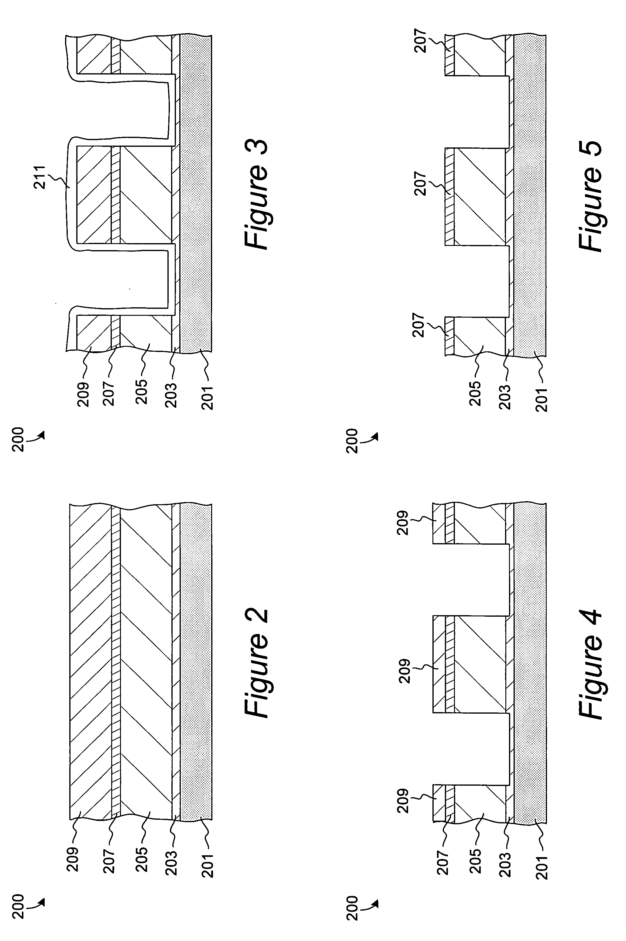
[0022]In the following detailed description of the present invention, numerous specific embodiments are set forth in order to provide a thorough understanding of the invention. However, as will be apparent to those skilled in the art, the present invention may be practiced without these specific details or by using alternate elements or processes. For example, specific methods described below reference removal of photoresist, etchant residues, and various polymeric materials left on a wafer after etching device features on a wafer using photoresist / lithography / etch techniques. However, the invention is not limited to cleaning these specific materials from a wafer. Additionally, the gas mixtures used to generate plasmas as described herein are provided for exemplary description of the invention. In some instances well-known processes, procedures, and components have not been described in detail so as not to unnecessarily obscure aspects of the present invention.

[0023]The following de...


PUM

PropertyMeasurementUnit
Temperatureaaaaaaaaaa

Abstract

The present invention pertains to methods for cleaning semiconductor wafers, more specifically, for removing polymeric and other residues from a wafer using dry plasmas generated with microwave (MW), electromagnetic field (inductively-coupled plasma (ICP)), and radio frequency (RF) energy. First, a wafer is treated by applying a microwave-generated plasma or an inductively-coupled plasma. Second, a radio frequency generated plasma is applied. Each of the microwave-generated plasma and the inductively-coupled plasma is produced from a gas mixture, which includes an oxygen source gas, a fluorine source gas, and a hydrogen source gas. Using such plasmas provides more controllable etch rates than conventional plasmas via control of fluorine concentration in the plasma. Application of a radio frequency generated (preferably oxygen-based) plasma is used for additional photoresist and polymer removal. The use of this two-step approach provides superior wafer cleaning compared to conventional wet and dry clean methods.

Description

FIELD OF THE INVENTION[0001]The present invention pertains to methods for cleaning or surface treatment of semiconductor wafers. More specifically, the invention pertains to methods for removing polymeric and other residues from a wafer using dry plasmas generated with microwave (MW), electromagnetic field (inductively-coupled plasma (ICP)), and radio frequency (RF) energy. The invention is applicable to Damascene and other integrated circuit fabrication processing.BACKGROUND OF THE INVENTION[0002]Photoresist strip and residue removal are critical in integrated circuit (IC) fabrication. During polysilicon etching in a typical integrated circuit fabrication process, undesirable etch residues and / or polymers such as hydrocarbon, oxide and / or silicon residues (e.g. SixBrxClxOx) may be formed and left on the surfaces and sidewalls of the resulting polysilicon structure. Such undesirable residues along with the remaining post-etch photoresist must be removed to prevent oxidation quality ...

Claims


Application Information

Patent Timeline
IPC IPC(8): B08B7/04B08B7/00
CPCB08B7/0035H01J37/32192H01L21/02071H01L21/31138H01J2237/335
Inventor CHIU, EDDIECHEN, CINDY WAILAMSU, YUH-JIAGRAFF, WESLEY PHILLIP
Owner NOVELLUS SYSTEMS
Why Eureka
Try Eureka