

Atomic layer deposition methods for forming a multi-layer adhesion-barrier layer for integrated circuits
- Summary
- Abstract
- Description
- Claims
- Application Information
AI Technical Summary
Benefits of technology
Problems solved by technology
Method used
Image

Examples
example 1
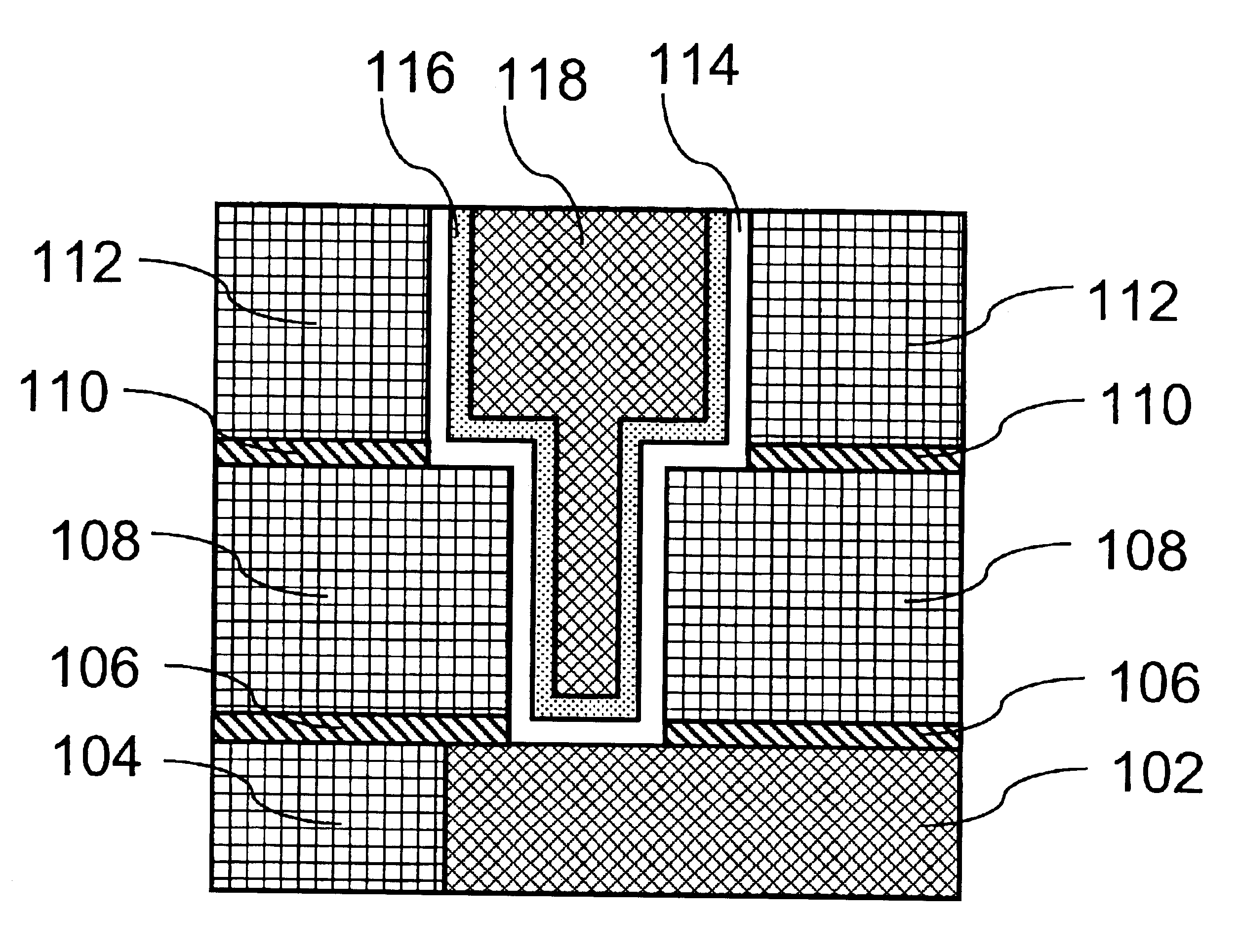
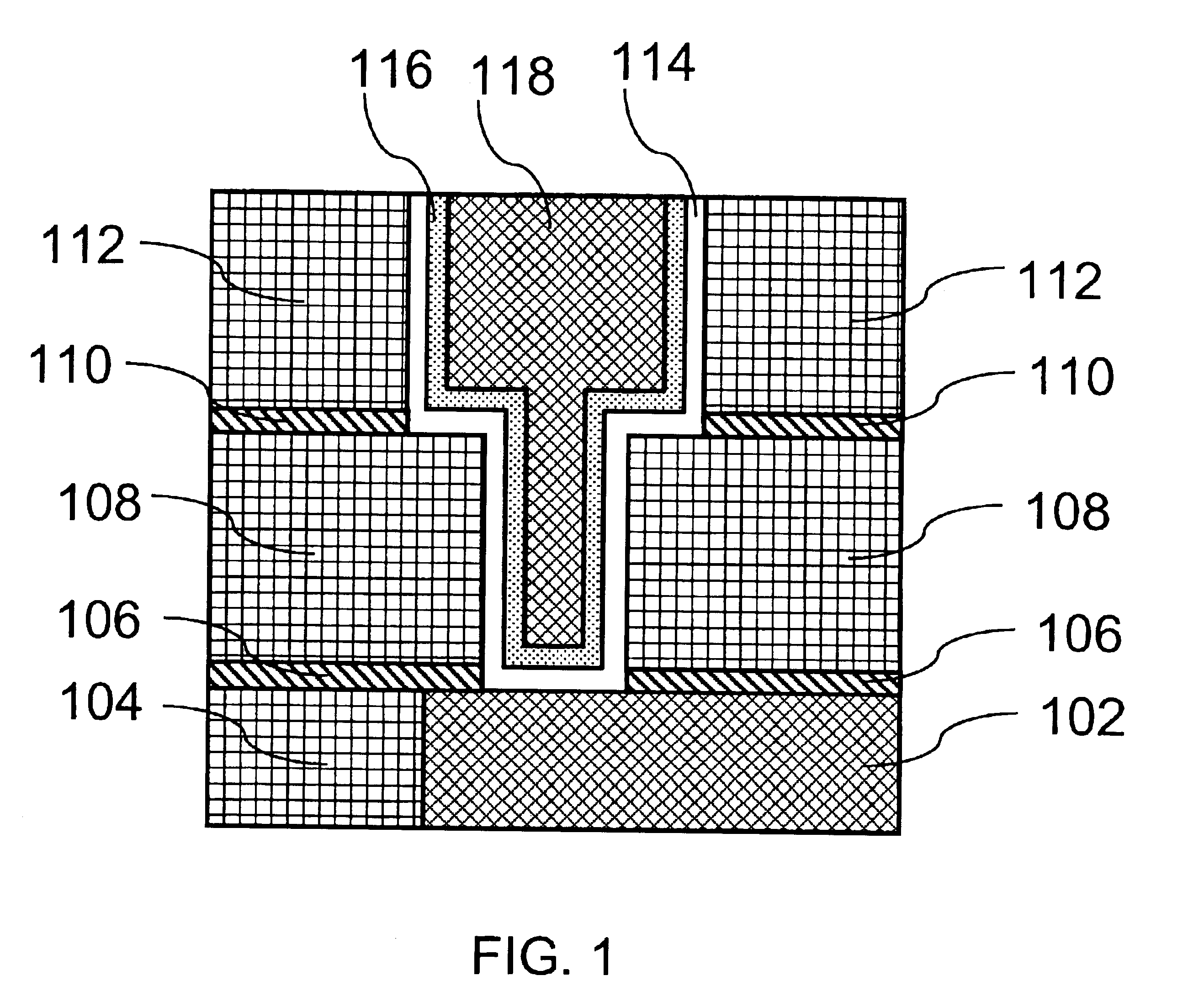
[0041]An example of a process for producing a layer that acts as a barrier layer, an adhesion layer and a seed layer in an IC is provided below. The duration (s) and approximate mass flow rate (sccm)of each pulse are given in parentheses.[0042]Step 1:
[0043]Repeat 20 deposition cycles of ALD to produce about 15 Å thick WNxCy barrier layer. One deposition cycle contains precursor pulses and purging pulses and one cycle can be written as:[0044]Introduce a pulse (0.2 s, 30 sccm) of gaseous WF6 carried with Ar (300 sccm) into the reaction chamber provided with the substrate; introduce an Ar purging pulse (1 s, 300 sccm); introduce a pulse (0.5 s, 50 sccm) of NH3 carried with Ar (300 sccm); introduce an Ar purging pulse (1s, 300 sccm); introduce a pulse of triethyl boron (TEB) by passing an Ar flow through a TEB container (1 s, 300 sccm); introduce an Ar purging pulse (1 s, 300 sccm).[0045]Step 2:
[0046]Repeat 10 deposition cycles of PEALD to produce a layer of W about 3 Å thick. One depos...
example 2
[0055]A process for producing a structure according to a preferred embodiment of the present invention can be presented as following:[0056]Step 1:
[0057]Repeat 5 times a sequence of 10 cycles PEALD TaN+10 cycles PEALD Ta to produce a barrier layer of Ta / TaN about 25 Å thick.
[0058]One cycle of PEALD TaN can be written as:[0059]Introduce a pulse of gaseous TaF5 with Ar passing through heated (150° C.) TaF5 container into the reaction chamber provided with a substrate (0.5 s, 300 sccm); introduce an Ar purging pulse (1 s, 300 sccm); introduce a H2 / N2 / Ar plasma pulse over the substrate (2 s, 300 sccm), introduce an Ar purging pulse (1 s, 300 sccm).
[0060]One cycle of Ta can be written as:[0061]Introduce a pulse of gaseous TaF5 (0.5 s); introduce an Ar purging pulse (1 s); introduce a H2 / Ar plasma pulse over the substrate (2 s); introduce an Ar purging pulse (1 s).[0062]Step 2:
[0063]Repeat 10 times a sequence of 1 cycle PEALD Cu+1 cycle PEALD Ta to produce a nanolaminate layer about 5 Å th...
example 3
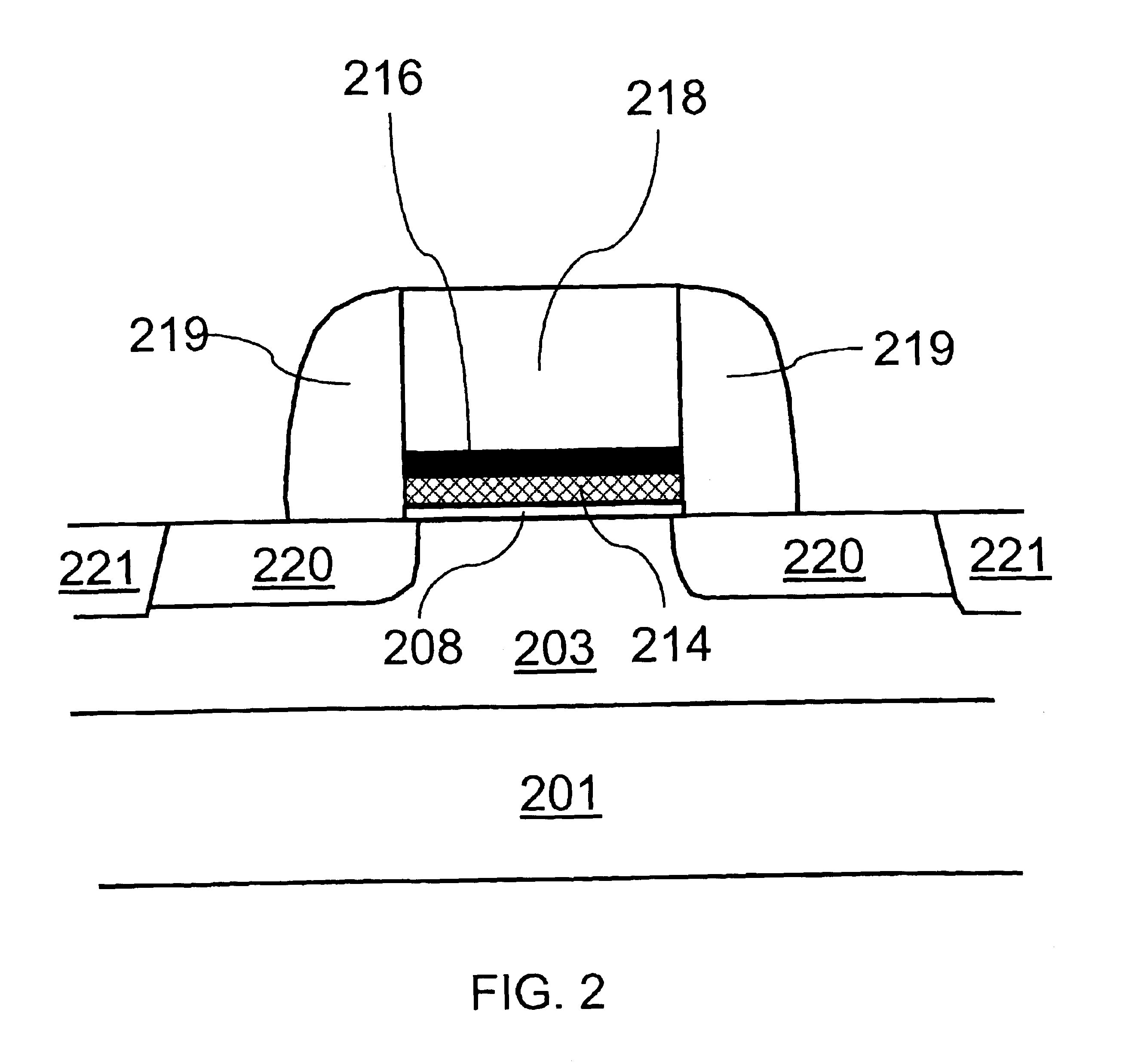
[0077]First, a barrier layer is formed over the dielectric layer of an IC. 20 deposition cycles of ALD are repeated to form a WNxCy layer, the thickness of which layer is about 15 Å. In one deposition cycle a WF6 pulse with duration of 0.2 seconds is introduced into a reaction chamber provided with the substrate containing the IC, an Ar purging pulse with duration of 1 second is introduced, a NH3 pulse with duration of 0.5 seconds is introduced, an Ar purging pulse with duration of 1 second is introduced, a triethyl boron (TEB) pulse with duration of 1 second is introduced, and an Ar purging pulse with duration of 1 second is introduced. The temperature of the reaction chamber is constant and set to a value selected from a range of about 150° C.-400° C. The pressure of the reactor is below room pressure, preferably selected from a range of about 0.1-10 mbar.
[0078]Second, a layer of metal alloy is formed over the barrier layer either in the same reaction chamber as the diffusion barr...
PUM
 Abstract
Description
Claims
Application Information