Optical waveguide type optical modulator and production method therefor

a technology of optical modulator and optical waveguide, which is applied in the direction of optical waveguide light guide, instruments, optics, etc., can solve the problems of accelerated penetration of resist components into the buffer layer, contamination of the buffer layer, and amine-based compound contamination, so as to prevent the leakage of electric current applied to the electrode caused by contaminants on the surface or inside of the buffer layer, and achieve excellent operation stability. , the effect of preventing the effect of leaking the electric current applied to th

Inactive Publication Date: 2005-10-18
SUMITOMO OSAKA CEMENT CO LTD
View PDF28 Cites 30 Cited by
  • Summary
  • Abstract
  • Description
  • Claims
  • Application Information

AI Technical Summary

Benefits of technology

[0027]A method of manufacturing such an optical waveguide type optical modulator comprises a process for forming optical waveguides on the surface of a ferroelectric substrate, which is made of a single crystal having an electro-optic effect, and the axis inducing an electro-optical effect is orthogonal to the main surface; a process for forming a buffer layer on the side of the ferroelectric substrate on which the optical waveguides are formed; a process for forming an electrically insulating protective film with a thickness of 50 to 200 nm on the buffer layer, at least in those regions excluding an electrode forming region; and a process for forming electrodes in the electrode forming region.
[0028]Furthermore, in the method of manufacturing the optical waveguide type optical modulator described above, the protective film is preferably formed after performing heat treatment, which the ferroelectric substrate having the buffer layer is heated in a film deposition apparatus. The buffer layer in this optical waveguide type optical modulator sometimes adsorb moisture during the interval between the buffer layer formation and the protective film formation, which has a negative effect on the stability of the operation of the optical waveguide type optical modulator. In particular, if the density of the buffer layer is low, then the buffer layer adsorbs moisture from the atmosphere quite easily.
[0029]According to the method of manufacturing an optical waveguide type optical modulator described above, because the ferroelectric substrate having the buffer layer undergoes heat treatment in the film deposition apparatus preceding the formation of the protective film even if the buffer layer adsorbs moisture during the interval between the buffer layer formation and the protective film formation, this moisture can be removed by the heat treatment. Accordingly, an opt

Problems solved by technology

However, when the signal field adjustment region is formed on the buffer layer using a lift-off method, because the photoresist is applied directly to the buffer layer and hardened, the principal components and the diluent which constitute the photoresist may penetrate the buffer layer, causing contamination of the buffer layer.
In particular, if the buffer layer is silicon oxide, the surface of the buffer layer is sometimes treated with vapor of an amine-based compound in order to improve the adhesive strength of the photoresist to the silicon oxide, and in such a case, the buffer layer can also be contaminated by the amine-based compound.
Consequently, there is a danger that the penetration of the resist components into the buffer layer may be accelerated because components from the resist can dissolve in these solutions.
Moreover, these solutions may also be a source of contamination themselves.
Furthermore, when the signal field adjustment region is formed using a wet etching method, there is a danger that the buffer layer is contaminated by contacting the etchant or the resist removal agent.
If the buffer layer is contaminated, DC drift in the optical waveguide type optical modulator is promoted by the presence of ions derived from the contaminants, thereby reducing the long-term reliability of the optical waveguide type optical modula

Method used


Image

  • Optical waveguide type optical modulator and production method therefor
  • Optical waveguide type optical modulator and production method therefor
  • Optical waveguide type optical modulator and production method therefor

Examples


example 1

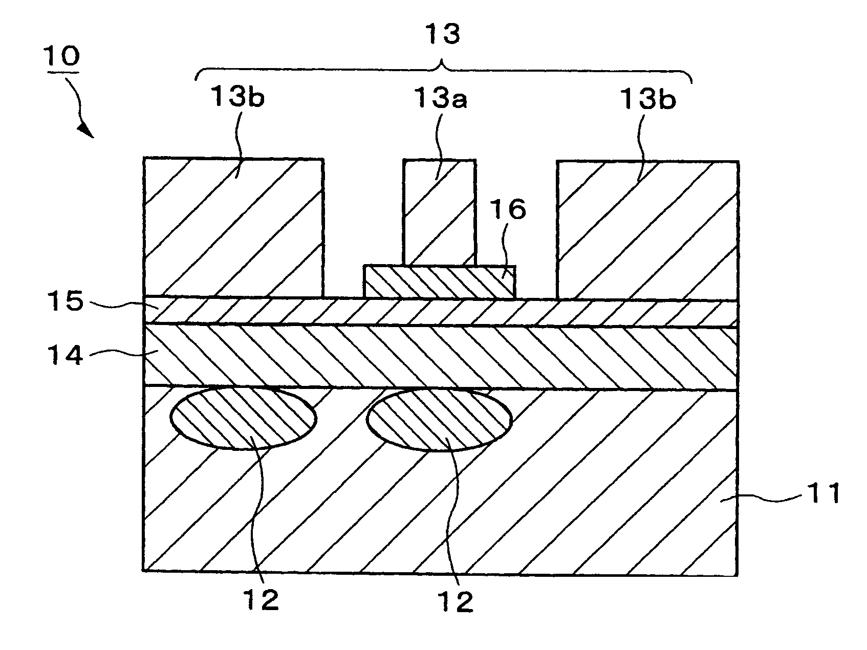
[0074]The optical waveguide type optical modulator 10 shown in FIG. 1 was manufactured in the following manner.

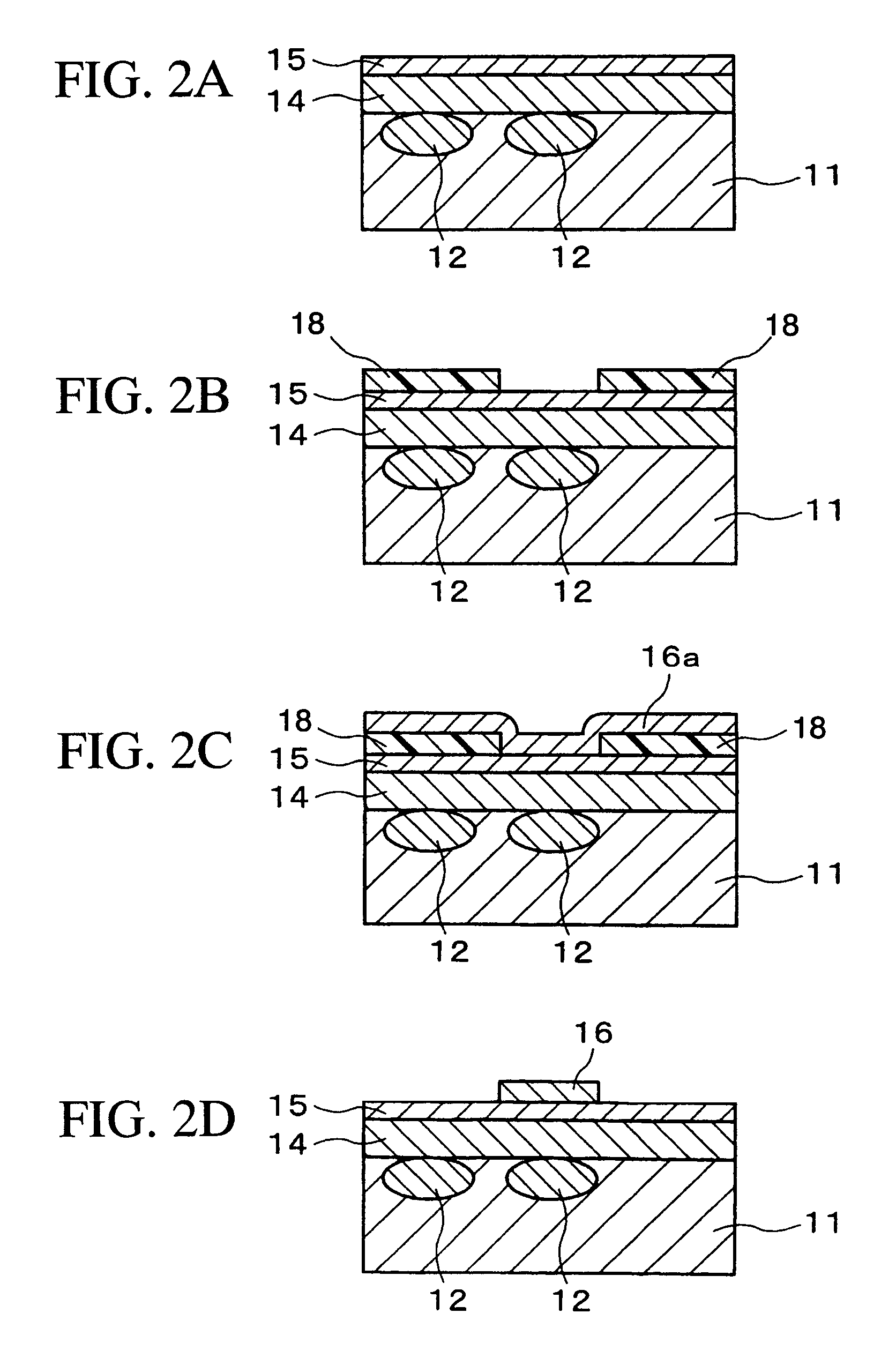
[0075]Optical waveguides 12 were formed on the surface of the ferroelectric substrate 11, which is made of lithium niobate, by performing diffusion processing of an optical waveguide pattern made of titanium having a thickness of 90 nm, for 15 hours under an oxygen atmosphere and at a temperature of 1000° C. A silicon oxide (SiO2) film with a thickness of 1000 nm, which forms the buffer layer 14, was then deposited on the substrate using a vacuum deposition method. After performing heat treatment at 500° C. in a stream of oxygen, a dielectric layer 15, which is made of silicon nitride and has a thickness of 100 nm, was formed on the entire surface of the buffer layer 14 by a sputtering method.

[0076]Then, after a photoresist was spin-coated on the entire surface of the dielectric layer 15 and subsequently hardened, a signal field adjustment region 16 was exposed onto the pho...

example 2

[0078]The optical waveguide type optical modulator 10 shown in FIG. 1 was manufactured in the same manner as in the example 1, with the exception that the dielectric layer 15 was formed of silicon oxynitride.

example 3

[0126]Optical waveguides 22 were formed on the surface of a ferroelectric substrate 21 made of Z-cut lithium niobate by performing a diffusion processing of an optical waveguide pattern made of Ti having a thickness of 90 nm, for 20 hours under an oxygen atmosphere and at a temperature of 1000° C. A SiO2 film with a thickness of 1 μm, which forms the buffer layer 23, was deposited on the substrate using a vacuum deposition method. After performing heat treatment at 600° C. for 5 hours in a stream of oxygen, an upper protective film 27 made of SiO2 having a thickness of 50 nm was formed on the entire surface of the buffer layer 23 by employing RF sputtering.

[0127]A transition metal layer made of Ti having a thickness of 50 nm, and an Au film having a thickness of 50 nm were formed sequentially on the protective film 27, using a vacuum deposition method within the same film deposition apparatus. A resist pattern was formed on the Au film using photolithographic techniques, and a thick...


PUM


Abstract

There is provided a high performance optical waveguide type optical modulator with excellent long term reliability, in which contamination of the buffer layer in a forming process of a signal field adjustment region on the buffer layer by a lift-off method or an etching method, is prevented and DC drift thus suppressed. The optical waveguide type optical modulator 10 comprises a substrate 11 having an electro-optic effect, optical waveguides 12 formed on the surface of this substrate 11, a traveling-wave type signal electrode 13a and ground electrodes 13b which are provided on the substrate 11 and control a lightwave, and a buffer layer 14 provided between the electrodes 13 and the optical waveguides 12, and furthermore, a dielectric layer 15 is provided on the entire surface of the buffer layer 14 on the side of the electrodes 13, and a signal field adjustment region 16 which has a wider width than that of the traveling-wave type signal electrode 13a and is made of a material with a higher refractive index than that of the dielectric layer 15 is formed between the dielectric layer 15 and the traveling-wave type signal electrode 13a.

Description

TECHNICAL FIELD[0001]The present invention relates to an optical waveguide type optical modulator suited to use in optical fiber communication systems and the like, and a manufacturing method thereof.BACKGROUND ART[0002]Recently, optical waveguide type optical modulators 140 as shown in FIG. 9 have become very common in optical fiber communication systems. In this optical waveguide type optical modulator 140, optical waveguides 142 are formed on a substrate 141 which has an electro-optic effect, and a guided lightwave which travels in he optical waveguides 142 is controlled by a traveling-wave type signal electrode 143a and grounded electrodes 143b. In the optical waveguide type optical modulator 140 of this example, normally, a buffer layer 144 made of an insulating material such as silicon oxide is formed on the substrate 141 to prevent absorption of the guided lightwave which travels in the optical waveguide 142 by the electrodes 143. Furthermore, a signal field adjustment region...

Claims


Application Information

Patent Timeline
IPC IPC(8): G02F1/01G02F1/035G02F1/225G02F1/03
CPCG02F1/0356G02F1/2255G02F2201/07G02F2202/42G02F2203/21
Inventor NAGATA, HIROTOSHIMIYAMA, YASUYUKIYAMAMOTO, FUTOSHISHINRIKI, TAKASHISHIMIZU, RYO
Owner SUMITOMO OSAKA CEMENT CO LTD
Why Eureka
Try Eureka