Semiconductor device and fabrication method thereof

a technology of semiconductor devices and capacitors, applied in the field of semiconductor devices, can solve the problems of reducing the accumulated capacity of capacitors, lowering the contrast of image displays, and high off currents, and achieve the effect of improving the operation performance and reliability of semiconductor devices

Inactive Publication Date: 2005-11-22
SEMICON ENERGY LAB CO LTD
View PDF46 Cites 74 Cited by
  • Summary
  • Abstract
  • Description
  • Claims
  • Application Information

AI Technical Summary

Benefits of technology

[0016]In order to solve the problems described above, the present invention aims at improving operation performance and reliability of a semiconductor device by optimizing the structures of the TFT used for each circuit of the semiconductor device in accordance with the function of each circuit.
[0017]It is another object of the present invention to provide a structure for lowering the area of a holding capacitance provided to each pixel and for improving an aperture ratio in a semiconductor device having a pixel unit.
[0019]In addition to the construction described above, the holding capacitance of the pixel unit may comprise a shading film arranged on a resin film, an oxide of the shading film and a pixel electrode. According to this arrangement, the holding capacitance can be formed with an extremely small area and consequently, the aperture ratio of the pixel can be improved.

Problems solved by technology

However, the poly-silicon TFT involves the problem that its OFF current is likely to become high.
It is believed that the main cause is hot carrier injection, and the hot carriers generated by a high field in the proximity of the drain presumably invite this degradation.
However, the accumulated capacity of this capacitor decreases gradually due to a leakage current resulting from the OFF current, or the like.
Consequently, the quantity of transmitting rays of light changes, thereby lowering the contrast of image display.
On the contrary, the ordinary LDD structures have a high effect for restricting the OFF current value, but is not resistant to hot carrier injection, as is well known in the art.
Particularly in the case of a small high precision panel used for a projector type display device, the area per pixel is so small that the drop of the aperture ratio by the capacitance wiring becomes a serious problem.

Method used


Image

  • Semiconductor device and fabrication method thereof
  • Semiconductor device and fabrication method thereof
  • Semiconductor device and fabrication method thereof

Examples


example 1

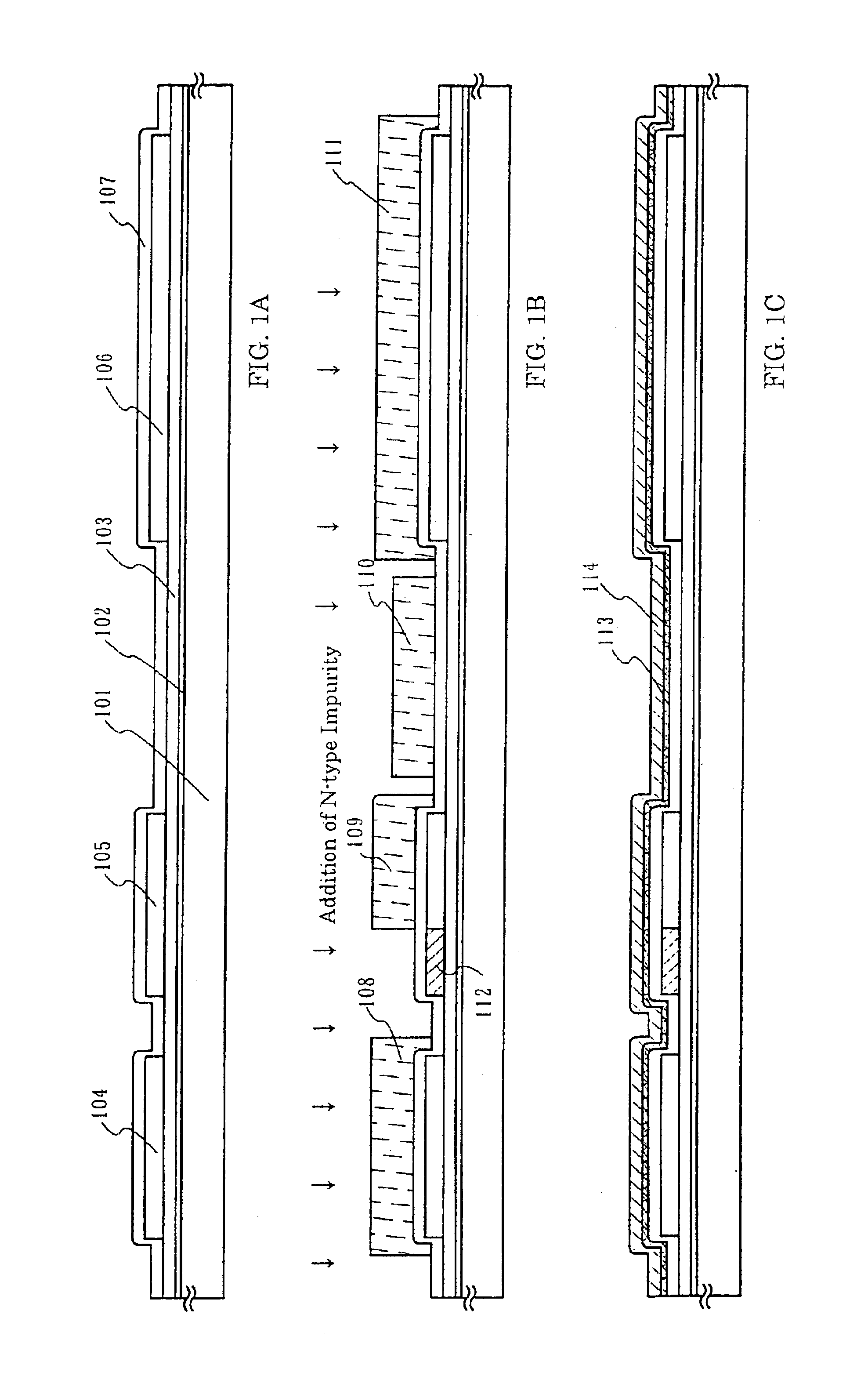
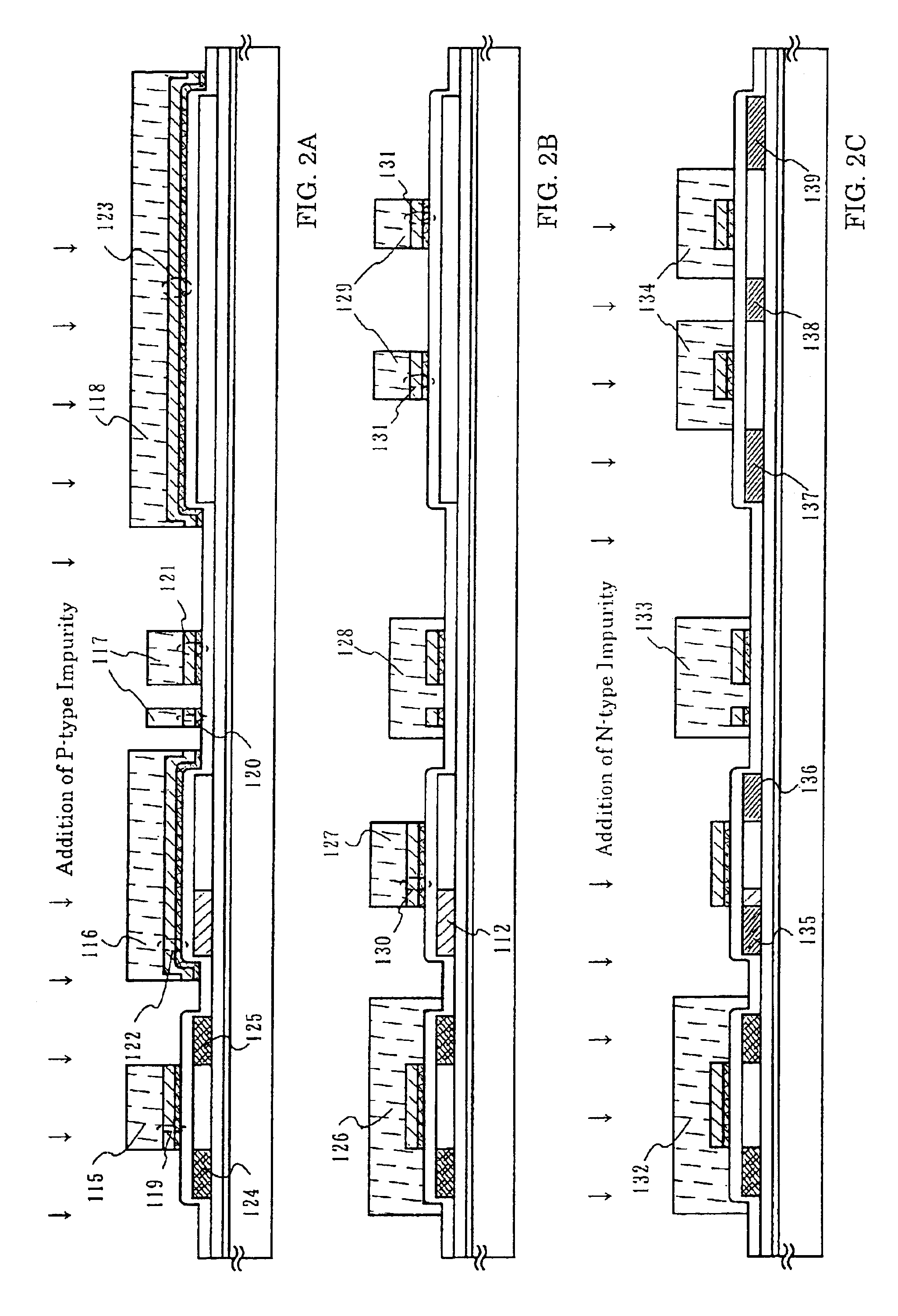
[0065]The first example will be explained with reference to FIGS. 1A to 1C, 2A to 2C and 3A to 3C. A method of simultaneously fabricating TFT of a pixel unit and TFT of a driving circuit disposed around the pixel unit will be explained.

[0066]FIG. 1A shows the formation step of active layers and a gate insulation film.

[0067]In FIG. 1A, a substrate 101 is preferably made of a glass substrate, a quartz substrate or a plastic substrate (inclusive of a plastic film). A silicon substrate or a metal substrate having an insulation film on the surface thereof can be used, too.

[0068]An underlying film 102 that comprises a silicon-containing insulation film (the term “insulation film” generically represents a silicon oxide film, a silicon nitride film and a silicon nitride oxide film in this specification) is formed by a plasma CVD process or a sputtering process to a thickness of 100 to 400 nm on the surface of the substrate 101 on which the TFTs are to be fabricated. The term “silicon nitrid...

example 2

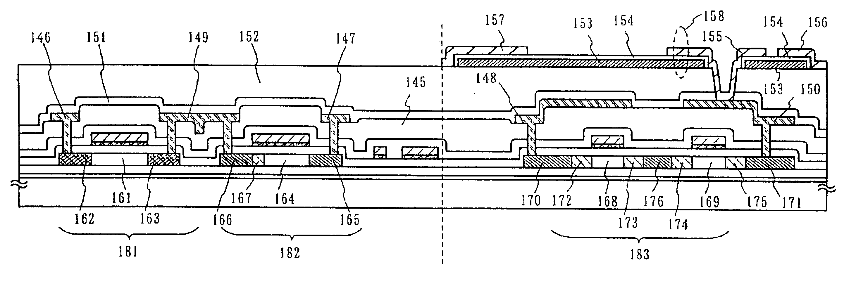
[0113]In this example, another structure of the holding capacitance connected to the n-channel TFT 401 of the pixel unit of the active matrix substrate will be explained with reference to FIG. 4. Incidentally, the sectional structure shown in FIG. 4 is entirely the same as that of Example 1 up to the process step of forming the oxide 154, and the structure up to this step has been explained already with reference to FIGS. 1A to 1C, 2A to 2C and 3A to 3C. Therefore, only the difference of this example from Example 1 will be explained.

[0114]After the shading film 153 and the oxide 154 obtained by oxidizing the shading film 153 are formed in accordance with the process steps of Example 1, spacers 402, 403 and 404 comprising an organic resin film a reformed. A film selected from the group consisting of polyimide, polyamide, polyimideamide, acrylic and BCB (benzocyclobutene) can be used for the organic resin film. Thereafter, the spacer 402, the second inter-layer insulation film 152 and...

example 3

[0117]In this example, still another structure of the holding capacitance connected to the n-channel TFT of the pixel unit of the active matrix substrate will be explained with reference to FIGS. 5A to 5C. Incidentally, the sectional structure shown in FIGS. 5A to 5C is exactly the same as that of Example 1 up to the process step of forming the shading film 153, and the structure up to this process step has been explained already with reference to FIGS. 1A to 1C, 2A to 2C and 3A to 3C. Therefore, only the difference of this example from Example 1 will be explained.

[0118]After the shading film 153 is formed in accordance with the process steps of Example 1, spacers 501, 502 and 503 comprising an organic resin film are formed in such a manner as to cover the end portions of the shading film 153. A film selected from the group consisting of polyimide, polyamide, polyimideamide, acrylic and BCB (benzocyclobutene) can be used for the organic resin film (FIG. 5A).

[0119]Next, an oxide 504 ...


PUM

PropertyMeasurementUnit
current consumptionaaaaaaaaaa
thicknessaaaaaaaaaa

Abstract

This invention provides a semiconductor device having high operation performance and high reliability. An LDD region 707 overlapping with a gate wiring is arranged in an n-channel TFT 802 forming a driving circuit, and a TFT structure highly resistant to hot carrier injection is achieved. LDD regions 717, 718, 719 and 720 not overlapping with a gate wiring are arranged in an n-channel TFT 804 forming a pixel unit. As a result, a TFT structure having a small OFF current value is achieved. In this instance, an element belonging to the Group 15 of the Periodic Table exists in a higher concentration in the LDD region 707 than in the LDD regions 717, 718, 719 and 720.

Description

BACKGROUND OF THE INVENTION[0001]1. Field of the Invention[0002]This invention relates to a semiconductor device having a circuit comprising thin film transistors (hereinafter referred to as “TFTs”) on a substrate having an insulation surface, and to a fabrication method of such a semiconductor device. More specifically, the present invention relates to electro-optical apparatuses (called also “electronic appliances”) typified by a liquid crystal display device including a pixel unit (pixel matrix circuit) and driving circuits (driver circuits) disposed around the pixel unit and formed on the same substrate and an EL (Electro-Luminescence) display device, and electrical appliances (called also “electronic appliances”) having the electro-optical apparatus mounted thereto.[0003]The term “semiconductor device” used in this specification represents generally those apparatuses which function by utilizing semiconductor characteristics, and includes also the electro-optical apparatuses and...

Claims


Application Information

Patent Timeline
Patent Type & Authority Patents(United States)
IPC IPC(8): G02F1/1362G02F1/13H01L29/786H01L29/66H01L21/70H01L27/12H01L21/84G09F9/30G02F1/136G02F1/1368H01L21/336H01L21/77H01L27/32H01L51/50H05B44/00
CPCG02F1/13454H01L27/12H01L29/458H01L29/78621H01L27/1248H01L29/78675G02F1/136286H01L27/124H01L29/78627H01L2029/7863H10K59/123H10K59/124H10K59/126H10K59/131H10K59/1213H10K59/1201G02F1/133345G02F1/136227G02F1/1368G02F2201/123G02F2202/104H01L27/1222H01L27/1259
Inventor YAMAZAKI, SHUNPEIMURAKAMI, SATOSHIKOYAMA, JUNTANAKA, YUKIOKITAKADO, HIDEHITOOHNUMA, HIDETO
Owner SEMICON ENERGY LAB CO LTD
Why Eureka
Try Eureka