Method for fabricating a semiconductor structure

Inactive Publication Date: 2005-11-22
POLARIS INNOVATIONS
View PDF6 Cites 5 Cited by
  • Summary
  • Abstract
  • Description
  • Claims
  • Application Information

AI Technical Summary

Benefits of technology

[0008]It is an object of the present invention to provide a method for fabricating a semiconductor structure having a plurality of gate stacks on a se

Problems solved by technology

Both have appeared to be impossible heretofore in the cell array.
On the one hand, siliconizations are not used at the present time in the DRAM selection transistor array for cost reasons.
High dopant concentrations in the source/drain region, on the other hand, lead, in the case of transistors having structural dimensions of smaller than 200 nm, to high dopant gradients which result in high electric fields between the source/drain region and an underlying well region.
High electric fields in turn cause increased leakage currents and thus short retention times of the signal or level stored in the memory cell.
A large connection resistance, which is essentially composed of the contact res

Method used


Image

  • Method for fabricating a semiconductor structure
  • Method for fabricating a semiconductor structure
  • Method for fabricating a semiconductor structure

Examples


Example

[0035]In the figures, identical reference symbols designate identical or functionally identical constituent parts.

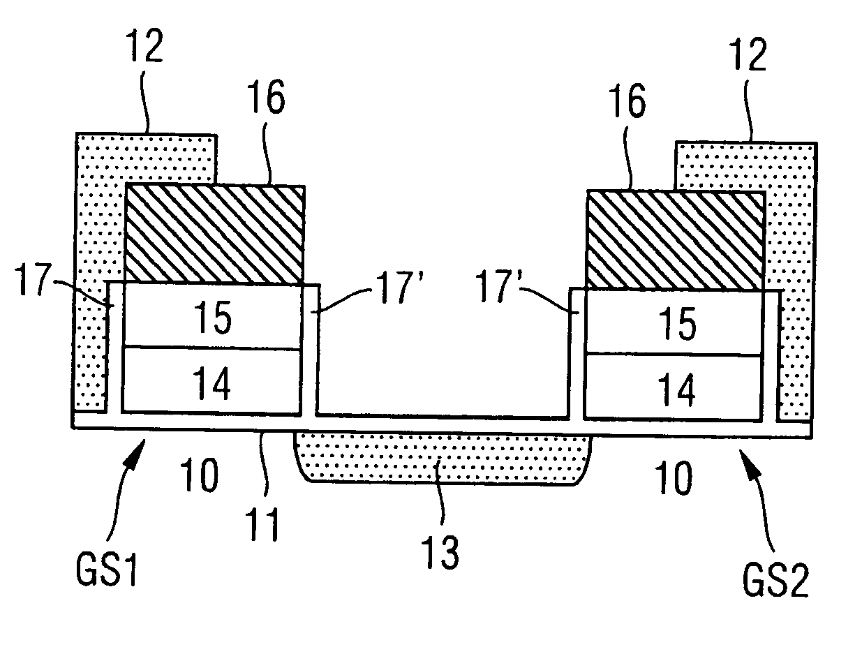
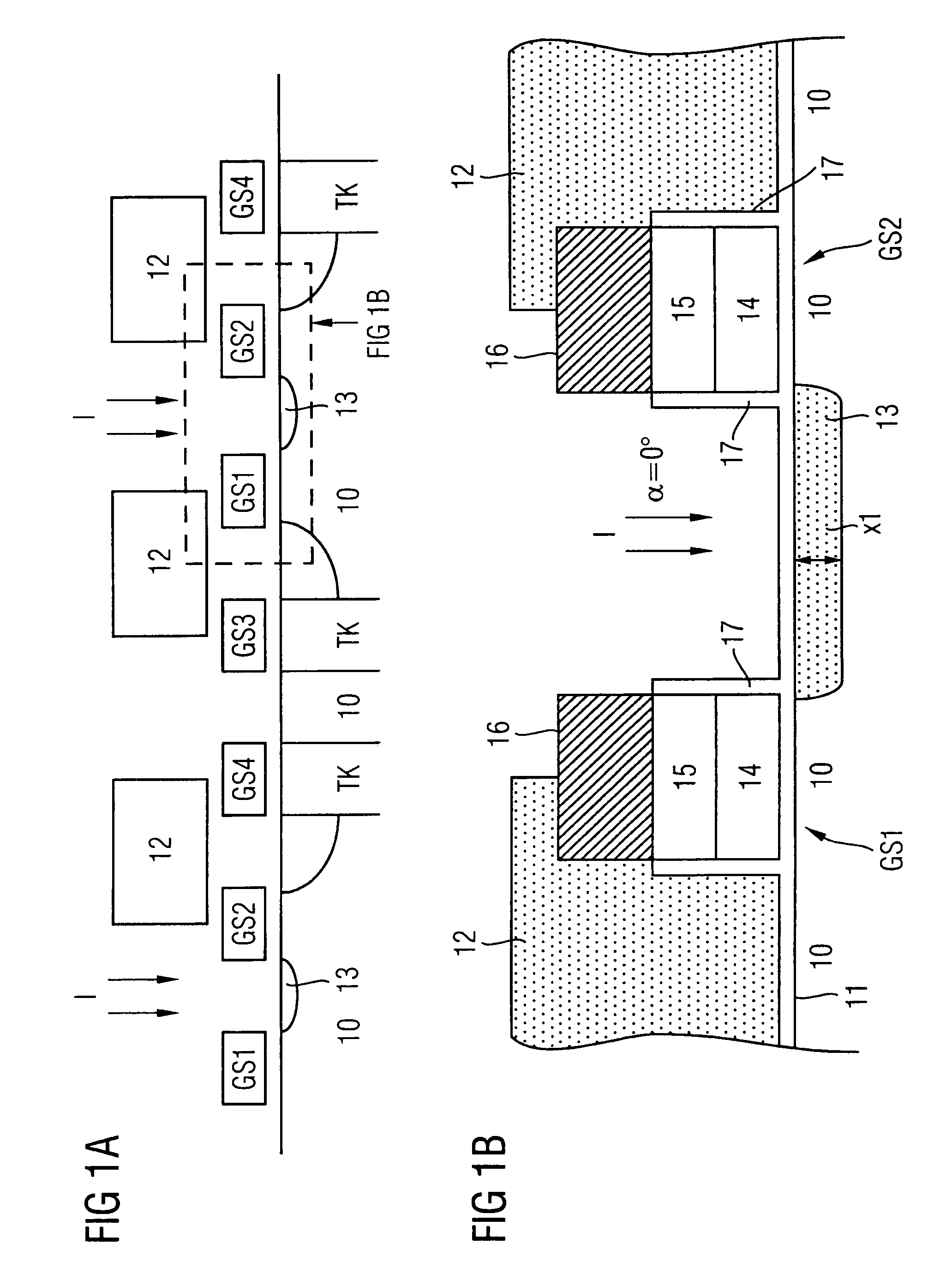
[0036]FIG. 1A diagrammatically illustrates a cross section of a DRAM semiconductor structure in a larger detail. A plurality of gate stacks GS1, GS2, GS3 and GS4 are arranged, preferably equidistantly, on a semiconductor substrate 10, a storage capacitor TK for storing an information item, i.e. an electrical charge, being arranged below every third or first gate stack GS3, GS4 in a cross-sectional plane. The gate stacks GS1 to GS4 are preferably patterned identically, provided in a plurality and are described in more detail with reference to FIG. 1B. A mask 12 is illustrated diagrammatically above the interspace between the gate stack GS3 and GS1 and between GS2 and GS4, so that the region between the gate stack GS1 and the gate stack GS2 is not covered by the mask 12 and an implantation I can be effected there, so that a section 13 provided with a doping is formed in th...


PUM


Abstract

The present invention provides a method for fabricating a semiconductor structure having a plurality of gate stacks (GS1, GS2, GS3, GS4) on a semiconductor substrate (10), having the following steps: application of the gate stacks (GS1, GS2, GS3, GS4) to a gate dielectric (11) above the semiconductor substrate (10); formation of a sidewall oxide (17) on sidewalls of the gate stacks (GS1, GS2, GS3, GS4); application and patterning of a mask (12) on the semiconductor structure; and implantation of a contact doping (13) in a self-aligned manner with respect to the sidewall oxide (17) of the gate stacks (GS1, GS2) in regions not covered by the mask (12).

Description

TECHNICAL FIELD[0001]The present invention relates to a method for fabricating a semiconductor structure and, in particular, to a method for fabricating a semiconductor structure having a plurality of gate stacks on a semiconductor substrate.BACKGROUND ART[0002]In the fabrication of DRAM modules, the array contacts are typically etched only after the deposition of an ILD layer or mask in the fabrication process. If metallic bit line contacts, for example a tungsten contact on silicon (CB), are then used, a contact hole implantation is additionally required for lowering the contact resistance between the semiconductor material and the metal. This implantation requires a separate photolithographic mask step, in which, after the etching of all the contact holes (not only the CB contact holes), all the other contact holes, such as CSN and CSP, in the peripheral circuits are covered and, consequently, only the CB contact holes are not covered by the mask and are thus accessible for the i...

Claims


Application Information

Patent Timeline
IPC IPC(8): H01L21/70H01L21/8242H01L21/8238H01L21/265H01L21/285H01L21/336
CPCH01L21/26586H01L21/28512H01L27/10888H01L29/66659H10B12/485
Inventor AMON, JURGENFAUL, JURGENGRUENING, ULRIKEJAKUBOWSKI, FRANKSCHUSTER, THOMASSTRASSER, RUDOLF
Owner POLARIS INNOVATIONS
Why Eureka
Try Eureka