Information processing apparatus and semiconductor memory

a technology of information processing apparatus and semiconductor memory, which is applied in the direction of digital storage, basic electric elements, instruments, etc., can solve the problems of frequent battery change, inability to spontaneously retain data, and volatile dram, and achieve reliable data retention over a long period of time.

Inactive Publication Date: 2005-11-22
SONY CORP
View PDF8 Cites 15 Cited by
  • Summary
  • Abstract
  • Description
  • Claims
  • Application Information

AI Technical Summary

Benefits of technology

[0044]It is an object of the present invention to realize reliable data retention over a long period of time in a high-speed nonvolatile memory, and provide an optimum control method therefor.
[0057]Even if periodic refresh is performed during standby as in a DRAM, for example, a memory having the spontaneous data retention capability such as a ferroelectric memory or the like makes it possible to reduce frequency of the refresh by a few orders of magnitude. Further, power supply to the memory can be stopped at appropriate times during the nonuse, thereby preventing occurrence of so-called dark current, which is current consumed by only supplying current to the circuit.
[0058]Thus, a combination of the spontaneous data retaining capability of film, the periodic refresh, and intermittent power supply makes it possible to minimize power consumption at the time of standby and retain data reliably.
[0060]In this case, at a time of normal use of the apparatus including access to the memory cell, current is supplied from the first power supply terminal (main power supply). When the main power supply is turned off at a time of nonuse of the apparatus, the power sensing means senses a decrease in supply potential of the first power supply terminal, whereby the semiconductor memory goes into a mode of refresh by the refresh control means. In the refresh mode, refresh is periodically performed within the memory chip using current supplied from the second power supply terminal. In such a refresh operation, the memory needs to consume only a minimum current for data retention, and a memory having the spontaneous data storing capability such as a ferroelectric memory or the like, in particular, makes it possible to reduce the current to a very low value, as described above. Therefore, data can be retained safely over a sufficiently long period of time even with the backup power supply, which has a capacity much lower than that of the main power supply.
[0061]In the case of the ferroelectric memory cell, in particular, at a time of refresh, inverted data is first written after reading, and then normal data is written. Alternatively, in order to simplify the sequence and stabilize the operation, preferably “1” is first written after reading, and then “0” is selectively written to restore data. This is effective in preventing erroneous operation due to an imprint.

Problems solved by technology

However, DRAM is volatile and is therefore not able to retain data spontaneously.
Therefore, even while not used, the apparatus consumes a few mW of current during the standby, thus requiring frequent battery change and extra battery cost.
Therefore, the current consumption for data retention during standby of a DRAM included in such household electric appliances is becoming a serious problem.
Therefore, the data retention of the high-speed nonvolatile memory is not so easy as that of a flash memory.
For example, a small defect in film caused in a manufacturing process makes a retention period by far shorter than an ideal retention period.
Nonvolatile memories generally ensure data retention for 10 years at 80° C. If the retention period is one day, a loss of data occurs in the memory, thus rendering the memory unusable.
Because of such a situation, it is very difficult to secure reliability of high-speed nonvolatile memories.
Such a condition considerably hinders progress toward higher integration and increases bit cost.
Therefore, the examples do not suppose long-term data retention during nonuse of the apparatus.
Even as for refresh at a time of turning on power, frequency of a user turning on the apparatus cannot be guaranteed nor be forced.
This method is very unreliable from a viewpoint of data retention during nonuse of the apparatus, and therefore cannot ensure long-term data retention.
Furthermore, in a ferroelectric memory, the same data stored over a long period of time causes internal movable charge to be redistributed and fixed so as to cancel an internal electric field attendant on polarization, causing a shift or distortion of the hysteresis loop.
This is referred to as an “imprint,” which in a bad case causes erroneous reading or erroneous writing.
During nonuse of the apparatus in this case, however, data is left as it is over an indefinite long period of time, so that a degree of deterioration of an imprint cannot be guaranteed.
That is, it is not possible to perfectly prevent the state of the imprint from deteriorating to such a degree as to cause erroneous reading.
Further, in that case, data is no longer restored even when refresh is performed because the data is lost at the time of reading.
This procedure is very complex and time-consuming.
Besides, when bit lines having a heavy capacitive load are inverted in the whole array, erroneous operation tends to be caused by occurrence of noise or the like.
Of course, this example is similar to the above examples in that it cannot be a sufficient measure against data retention degradation.

Method used


Image

  • Information processing apparatus and semiconductor memory
  • Information processing apparatus and semiconductor memory
  • Information processing apparatus and semiconductor memory

Examples


fourth embodiment

[0077]A first to the present invention will hereinafter be described, and thereafter a refresh sequence suitable for the embodiments will be described.

first embodiment

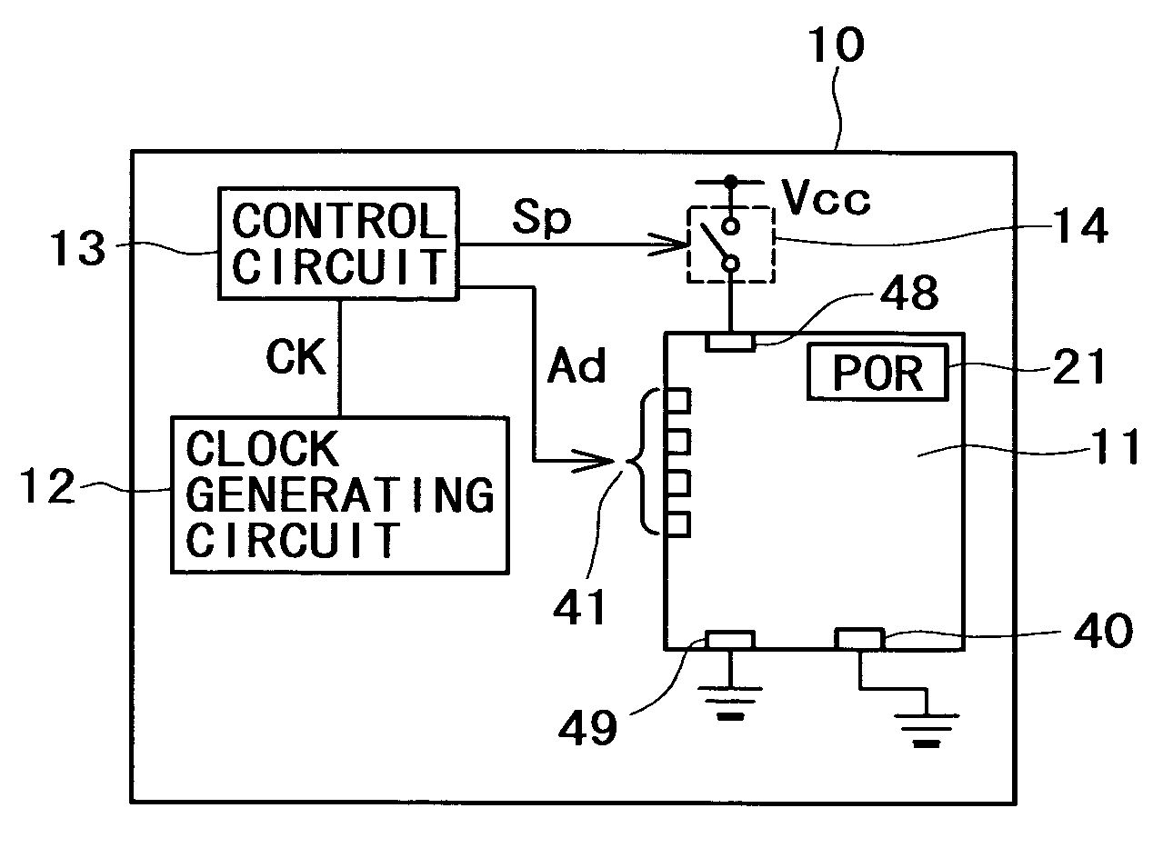
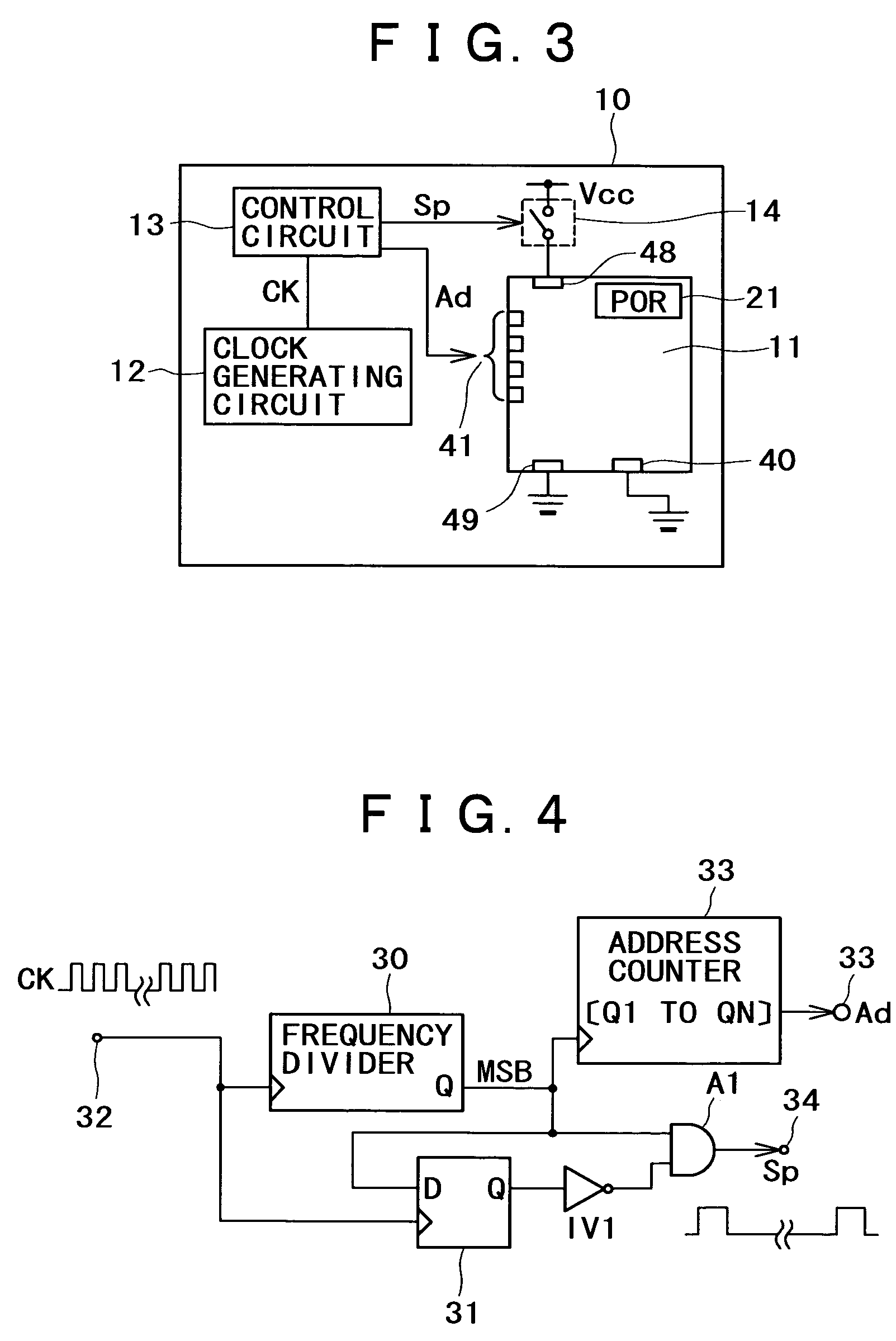
[0078]FIG. 3 shows a configuration of main parts of a FIG. 3 shows a memory chip 11 included in a computer apparatus (information processing apparatus) 10, and particularly shows a memory control configuration at a time of nonuse in the computer apparatus 10.

[0079]The time of nonuse of the apparatus specifically supposes that while a power supply switch of a user interface is turned off and the user does not communicate with the apparatus, the apparatus itself can be supplied with power as required via an internal battery or an adaptor to an external power supply.

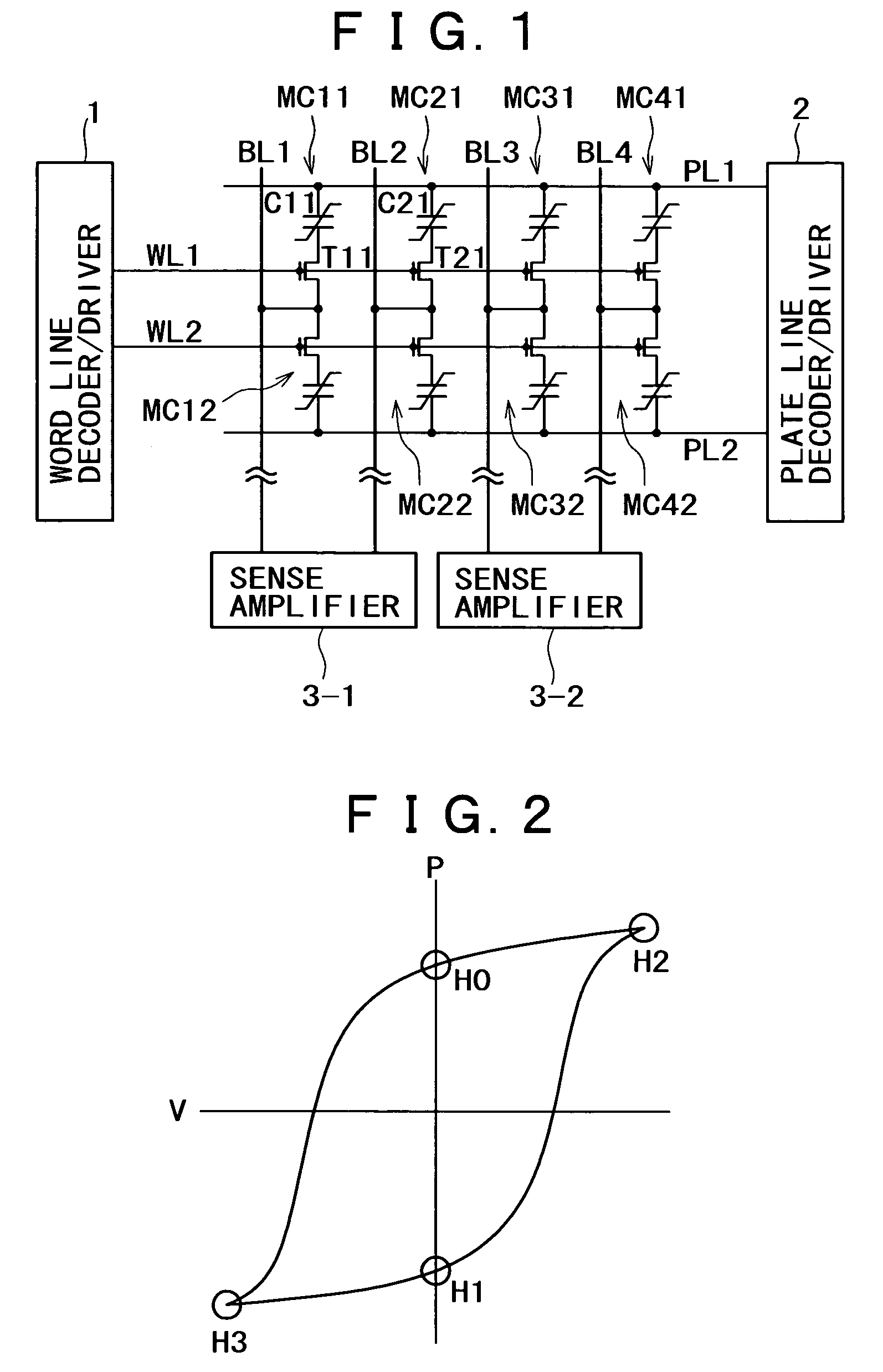
[0080]The memory chip 11 in this example includes a memory cell array as a ferroelectric memory and a circuit system for driving the memory cell array (a word line decoder / driver, a sense amplifier, a plate line decoder / driver, and the like) as described with reference to FIG. 1, for example.

[0081]The memory chip 11 is supplied with operating power from a power supply terminal 48. A ground terminal 49 is grounded.

[0082]In ...

third embodiment

[0135]FIG. 8 shows an example of circuit connection during standby of the memory chip 11c of the

[0136]The memory chip 11c has a power supply terminal 48 supplied with operating power Vcc.

[0137]A timer circuit 18 disposed within the memory chip 11c has functions of both the clock generating circuit 12 and the control circuit 13 in the first embodiment (FIGS. 3 to 5). The timer circuit 18 is supplied with current from the power supply terminal 48 at all times during standby. The timer circuit 18 is connected to a ground at all times by a ground terminal 49. The timer circuit 18 is thus operable during standby.

[0138]The timer circuit 18 outputs a power-on pulse Sp for periodic on / off control of power to a memory core 15c during standby. The timer circuit 18 also outputs an address signal Ad from an internal counter. The timer circuit 18 further supplies a refresh start timing signal RfS for the memory core 15c at appropriate times.

[0139]In addition, an inverter IV11 and a switch Q1 for...


PUM


Abstract

An information processing apparatus or a semiconductor memory according to the present invention periodically refreshes a high-speed nonvolatile memory cell having spontaneous data storing capability at the time of nonuse of the apparatus (or at the time of standby of the memory) by refresh control element. Thus, a combination of the spontaneous data retaining capability of the nonvolatile memory cell, the periodic refresh at the time of nonuse, and intermittent power supply by turning on / off a switch circuit makes it possible to retain data reliably while minimizing power consumption at the time of standby. Thereby a memory system that can retain data reliably with minimum power consumption and enable high-speed access can be realized.

Description

BACKGROUND OF THE INVENTION[0001]The present invention relates to a semiconductor memory and an information processing apparatus including the semiconductor memory.[0002]New semiconductor nonvolatile memories capable of high-speed rewriting have recently been drawing attention. The nonvolatile memories utilize various materials capable of changing a state at high speed with low voltage and retaining the state spontaneously.[0003]A typical example of the nonvolatile memories is a ferroelectric memory. A cell structure and operation of a currently mainstream ferroelectric memory are proposed in U.S. Pat. No. 4,873,664 of Patent Literature 1.[0004]FIG. 1 illustrates an example of a method of realizing the ferroelectric memory. In this example, a memory cell is formed by one access transistor and one ferroelectric capacitor, and 1 bit is stored by complementarily writing data to a pair of memory cells, for example.[0005]The example shown in FIG. 1 has memory cells MC11, MC21, MC31, MC41...

Claims


Application Information

Patent Timeline
Patent Type & Authority Patents(United States)
IPC IPC(8): G11C11/406G11C11/15G11C11/22
CPCG11C11/22G11C11/406G11C11/40615H04B7/24
Inventor NISHIHARA, TOSHIYUKI
Owner SONY CORP
Why Eureka
Try Eureka